On Sat, Sep 23, 2017 at 8:26 AM, Richard Wilbur
<richard.wil...@gmail.com> wrote:
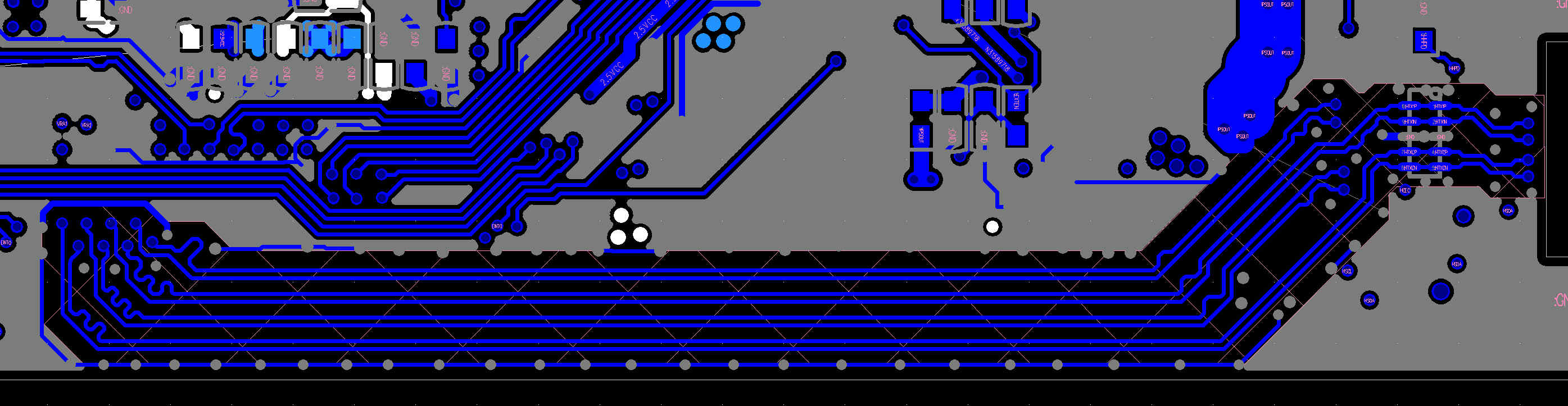
> After spending a couple minutes studying layers 3 and 4, here's what I see:
> 1.  It looks like there may be a difference in the signal via antipads on
> layers 3 and 4 and that would be a way for us to give just that handful of
> vias special properties--if need be--although in this case it interestingly
> looks like the antipads are larger on layer 4 than layer 3.  (optical
> illusion?)
> 2.  The (minimum?) polygon size or line width of the fill looks larger on
> layer 3 than layer 4.

 layer 4 HDMI vias are actually covered by VCC 3v3 flood-filled plane.
it's a 5mil clearance to that.  i decided i didn't like that, so i
made a cut-back in the 3V3 plane so that GND covers it instead.  it's
*still* 5mil even on that flood fill.

 so it's just something weird about the flood-fill on layer 3,
possibly due to it being a copper pour not a "plane area".  don't
know.  if absolutely necessary i can put in some tracks that split the
pairs.


> I think the second point, or something along those lines, likely explains the
> void on layer 3 and lack of void on layer 4.  It looks like if we were to
> find and adjust that fill parameter on layer 3, some of your explicit guard
> traces might become redundant. (I can see why you added them because the
> ground fill wasn't working as expected.)
>
> It would be nice to change layer 3 to make the signal path more uniform on
> the way through the vias but it's not the end of the world if we can't, as
> long as layers 2 and 5 resemble layer 4 in the vicinity of the HDMI
> differential signal vias adjacent to the A20.

 i have to use it as a signal layer, so there's tracks running round
the back of some of the diff-pair VIAs.

> The remaining questions are where do we impose 5mil clearance (by bringing in
> the fill), where do we start tapering, and what does the taper look like?
> Likewise, but in reverse order, at the other end.

 yehyeh

>>>>>>> Is the closest copper on layer 1, around the A20, 5mil from the HDMI
>>>>>>> differential signals?
>>>>>>
>>>>>> yes.  everything's 5 mil design rule.
>>>
>>> I agree that 5mil is the design rule.  The question is, "How close did
>>> we actually get?"  What I'm referring to as foreign copper is any
>>> trace, via, component land/pad, or fill that is not part of the
>>> differential pair under consideration.  In other words, did we make it
>>> from A20 land to via without getting closer than 10mil?  7mil?  We can
>>> adjust the proximity of ground fill with a manual keepout if we need
>>> more space so I'm not too worried about that.  I'm more curious about
>>> distance to other traces, lands/pads, or vias.
>>
>> ok - let me re-run the flood fill and do a quick review, starting from the
>> A20.
>>
>> so.  layer 1.  surrounded, all 5mil.  tracks are only 60mil or so to
>> the VIAs.  didn't do a keepout.  all 5mil.
>>
>> layer 3 (the VIAs) - some sort of curve on the flood-fill, it's 5mil
>> but there's a void in the middle.
>
> Are layers 2, 4, and 5 also 5mil away from the differential signal at the
> vias?

 yes.  layer 3 is the only exception.

>> layer 6, starts @ 5mil, expands out to 15mil (mostly).  exceptions:
>> distance to TX2 "long wiggle" is 7mil,  distance from bottom VIAs
>> along board edge (to TXC), 11.2mil, distance to track *between* the
>> VIAs 15mil.  distance to GND vias ABOVE the hdmi tracks (TX2), 19mil.
>>
>> in theory then i could move the entire set of horizontal tracks up
>> by... 4 mil... i reeaallly don't want to though as it means redoing
>> the whole f*****g lot of wiggles.... argh :)
>
> Can't select and move?

 you can... but there are special rules which ensure that 45 degree
angles on two adjacent segments are "respected".  it gets extremely
weird and extremely frustrating.

> Since it is such a long section it would be beneficial to move the traces.

 argh.  i kinda reached that conclusion :)

 what i can do to some degree is manually enter values (adding 4mil up
and 4 mil left/right) so that there's less to redo by hand.

> So if we bring in the keepout at 5mil on layer 6 and taper it slowly to 7mil
> by the point we get to the TX2 wiggle which exhibits 7mil clearance.  To make
> this work we have to start the pairs off around 5mil inter-pair spacing and
> then spread them as we taper the keepout.  I realize this is more complicated
> than what I first described.

 it's too much.  i can just about manage adding 4mil manually to every
single one of those long straights, moving them up from the 11mil
clearance to the bottom board-line VIAs to 15mil, thus taking 4mil off
that 19mil clearance and resulting in 15mil there as well.

 we don't have *room* for 7 mil inter-pair spacing.

 if i've misunderstood, do let me know.

>> yehhh there are so many GND vias at the ESD end i'd question its
>> effectiveness...
>
> You'd question the effectiveness of what?  The ESD component?  The taper?

 putting in a taper at the end is significantly disrupted by the
presence of non-removable VIAs.  you can *add* a taper... but then the
VIAs (which cannot be moved) are *already* within about 5mil or 7mil
of the tracks.

 what *would* work is bringing the taper in *BEFORE* the ESD
components.  it also coincides with the double 45-degree bending of
the group of tracks, so is still a bit... dodgy.

 see this picture for reference:
http://rhombus-tech.net/allwinner_a10/news/eoma68-a20-275-layer6-hdmi.jpg

 basically there's no point in tapering *after* the ESD components
because the GND vias are already closer than the taper would bring GND
in.

 l.

_______________________________________________
arm-netbook mailing list arm-netbook@lists.phcomp.co.uk
http://lists.phcomp.co.uk/mailman/listinfo/arm-netbook
Send large attachments to arm-netb...@files.phcomp.co.uk