At 02:25 PM 24/10/2018 -0700, you wrote:
>To draw out the schematics for the Displaywriter I have a bunch of boards to
>trace out,
>and I don't want to do the usual "scribble on yellow pad"
>to do it. Has someone written a graphical tool for doing this?
>
>What I would like to find is a tool that puts up a bunch of footprints with
>internal IC functions
>shown, then a way to rapidly enter the buzzed out interconnections, generating
>a netlist.
>
>This is exactly backwards workflow from normal schematic entry and pcb layout.
>
>I suspect I'm just going to have to bite the bullet and write it..
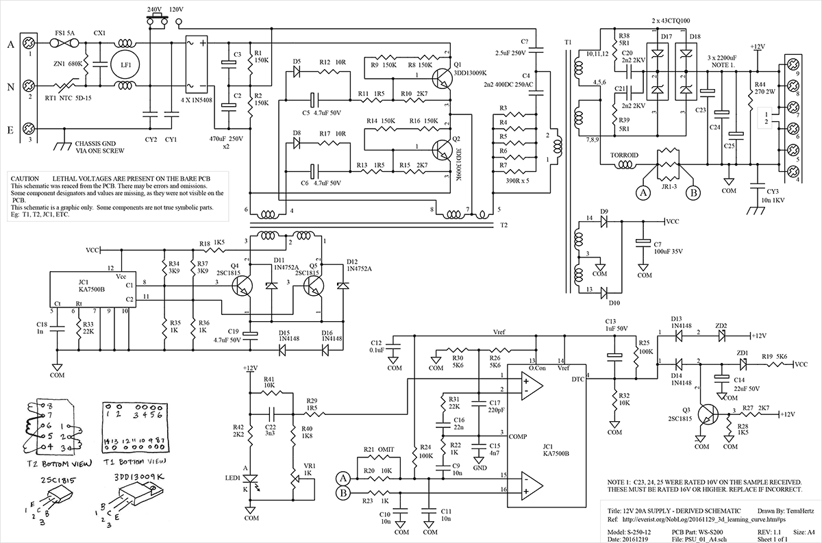
A: Yes. But god knows what it costs.

http://scancad.net/products/pcb-design-fabrication/pcb-reverse-engineering
ScanFAB is a fully integrated, stand-alone, scanner- based re-engineering
system that permits the creation of CAD data (DXF/Gerber/Drill/CNC) from
existing multilayer PCBs, parts, phototools, stencils, drawings, microfiche,
PDF files, X-Ray images, etc.
It also contains a full Gerber editor that can be used to import, modify and
export Gerber & Drill data.
ScanFAB uses Windows-based software linked to a high-resolution, calibrated
flatbed scanner. This combination allows for accurate reverse engineering and
precise reproduction of data to exact FORM, FIT and FUNCTION for today's high
density PCB board designs, complex parts and tooling.


Apart from that, here are some related discussions:
http://www.eevblog.com/forum/beginners/how-to-reverse-engineer-a-simple-through-hole-board/
How to reverse engineer a simple through-hole board

http://www.eevblog.com/forum/chat/making-reverse-engineered-altium-designs-public/
Making reverse engineered Altium designs public

And a few examples of my own reverse engineering for repairs:
http://everist.org/NobLog/20151112_planning_vacuum.htm#54120B_ps
http://everist.org/NobLog/20161129_3d_learning_curve.htm#ps
http://everist.org/NobLog/20160331_lightning_luck.htm#tla614

In general since I'm not trying to end up with schematics and PCB layouts for
remanufacture,
but just anything good enough for fault finding, I just use photoshop to aid in
the track
tracing stage. Then pencil and paper (in multiple stages) to end up with a
sensibly organized
schematic.
If I want a neat looking 'schematic' (just for viewing, ie only an image) I use
photoshop
for that too.  eg
http://everist.org/NobLog/pics/20161129/20161219_PSU_schem.png

Though to manufacture an identical or modified version of the thing, full
schematic editor
and layout CAD is necessary.


Btw Al, did you ever find that TM200 IBM card reader manual you recalled seeing
somewhere?
I still can't find a manual with schematics for my TM200. Plenty of M200
manuals, nothing for
the very different TM200.  See
http://everist.org/NobLog/20180922_data_in_holes.htm#tm200

Guy