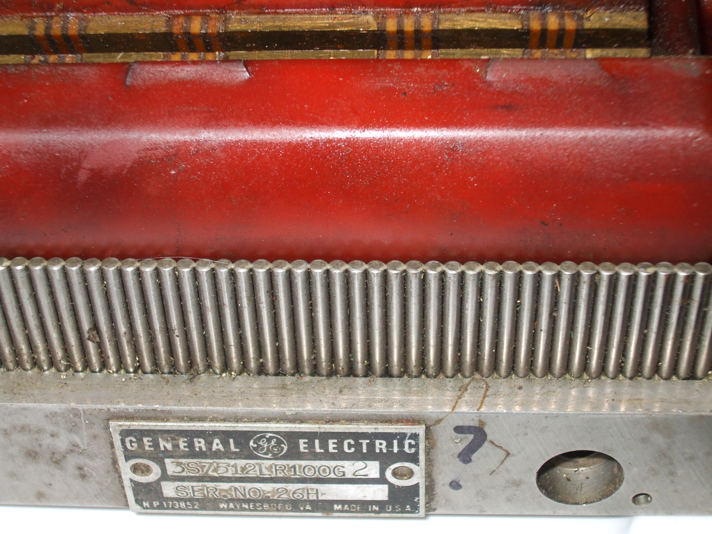
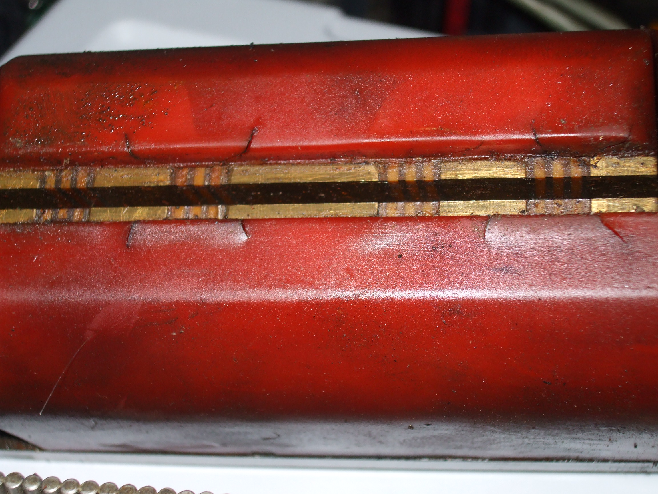
sam sokolik wrote:
> Here are some more pictures...  (top red thing is the read head)
> http://electronicsam.com/images/KandT/conversion/accpinset1.jpg
> http://electronicsam.com/images/KandT/conversion/accpinset.jpg
>
> This is how I understand it as of today.... ;)
>
> There are 4 coils - they are hooked up in a center tap config (see
> schem) - 2 sets of 2 coils. An excitation signal (250khz square wave) is
> sent to the outside connections of the 2 center tapped coils. The center
> taps are summed together and turned into a square wave. That square wave
> is shifted compared to the exciter signal depending on the position
> relative to the .1 pin.
>
> Now the way I think the controller did it was this - it had a 250khz
> clock - they used this to count the shift between the exciter signal and
> the summed square wave back from the center taps. this would give you
> 250khz/250hz - 1000 divisions within each pin.
>
Yup, that is about how I expected it would work, a very similar scheme
is used on some Farrand Inductosyns.
I think the Mesa resolver interface uses this scheme, too.  You should
check with them and see if they know how to make it work.  This is a
REALLLLY OLD encoder, too.  It sure doesn't look like it would be easy
to wire the existing read head to one of my resolver converters which
use the AD 2S1200 chip.
Jon

------------------------------------------------------------------------------
Download Intel® Parallel Studio Eval
Try the new software tools for yourself. Speed compiling, find bugs
proactively, and fine-tune applications for parallel performance.
See why Intel Parallel Studio got high marks during beta.
http://p.sf.net/sfu/intel-sw-dev
_______________________________________________
Emc-users mailing list
Emc-users@lists.sourceforge.net
https://lists.sourceforge.net/lists/listinfo/emc-users