DJ Delorie wrote:
>> Traces from the pin to be decoupled (bypassed) to teh cap should be as
>> short as possible and as fat as possible. Nothing wrong with making a
>> small plane out of that because it provides a small additional "courtesy
>> capacitance", for free, to the ground plane below.
>
> Comparison: http://www.delorie.com/electronics/powermeter/bypass-1.png
>
> The top is the "new" way, the bottom is the "old" way.
>
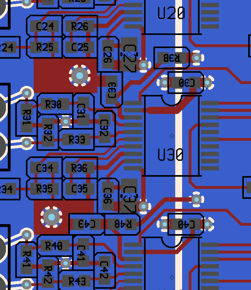
Better. You don't really need a plane at the GND side of C33 though. C30
is 1/2" away from the pin but not much you can do. Make the supply line
to pin 2 even fatter, heck, pour it all underneath the chip.


> I thought about adding a rectangle of copper under U30 tied to AVdd to
> act as a tiny cap, but I calculated it was only 0.2pF.  Maybe I'll use
> the space to add a big fat GND trace instead.
>

Yes, it ain't much. But free. However, I'd use the area to fatten up the
digital supply from C30 to pin 2 even more. Reduces the rattle at pin 2.
Can't see the schematic right now from your previous post because I
managed to screw up my Ubuntu a bit when I could not coax it to go full
screen in VirtualBox. Might need a re-install. Oh well, still learning.

--
Regards, Joerg

http://www.analogconsultants.com/

"gmail" domain blocked because of excessive spam.
Use another domain or send PM.


_______________________________________________
geda-user mailing list
[email protected]
http://www.seul.org/cgi-bin/mailman/listinfo/geda-user