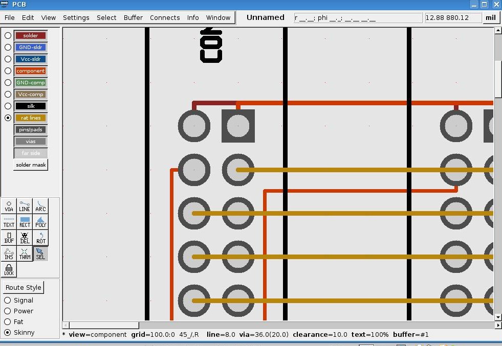
   I have a board I'm developing (maybe) that is a backplane.  It has 9
   edge connectors mounted on it and when I went to autoroute it Oh Lord!
   I've never seen such a mess!  Traces all over, a million or so vias,
   etc.  You'd think it would be a simple set of parallel lines, but no.
   So I ripped it up and started autorouting them one at a time.  The
   first one went well, then the second row didn't.  I'm guessing that I'm
   trying to violate some sort of clearance rule but I don't know which
   one or how to fix it.  I may even have the pins too large.  Take a look
   at the image
   [1]http://fayettedigital.com/images/board.jpg
   You can see the first pin in the second row shoots off towards the
   bottom of the board where it tries to go outside of the connector to
   connect to the second connector.
   It's a euroboard (32 pin).  The pin definitions from the footprint (my
   design) are all like:
           Pin[-10850 35000 7500 2000 9500 5200 "1" "1" "square"]
           Pin[-20850 35000 7500 2000 9500 5200 "2" "2" ""]
           Pin[-10850 45000 7500 2000 9500 5200 "3" "3" ""]
           Pin[-20850 45000 7500 2000 9500 5200 "4" "4" ""]
   I see boards all the time where traces run between the pins so I know
   it's done and I cannot believe someone has in each case done a manual
   layout.
   Thanks for any pointers.  The last time I had to lay up a pcb I used a
   drafting table, tee square and pen and ink.
   I think that was quicker.  ;)
   And if someone notices, yes I'm the same guy that was asking questions
   before but for some reason the mail list is not getting my postings any
   longer so I had to try from my gmail account.
   Jim.
References

   1. http://fayettedigital.com/images/board.jpg
_______________________________________________
geda-user mailing list
[email protected]
http://www.seul.org/cgi-bin/mailman/listinfo/geda-user