On Wed, 10 Nov 2010 16:57:33 -0500
DJ Delorie <[email protected]> wrote:
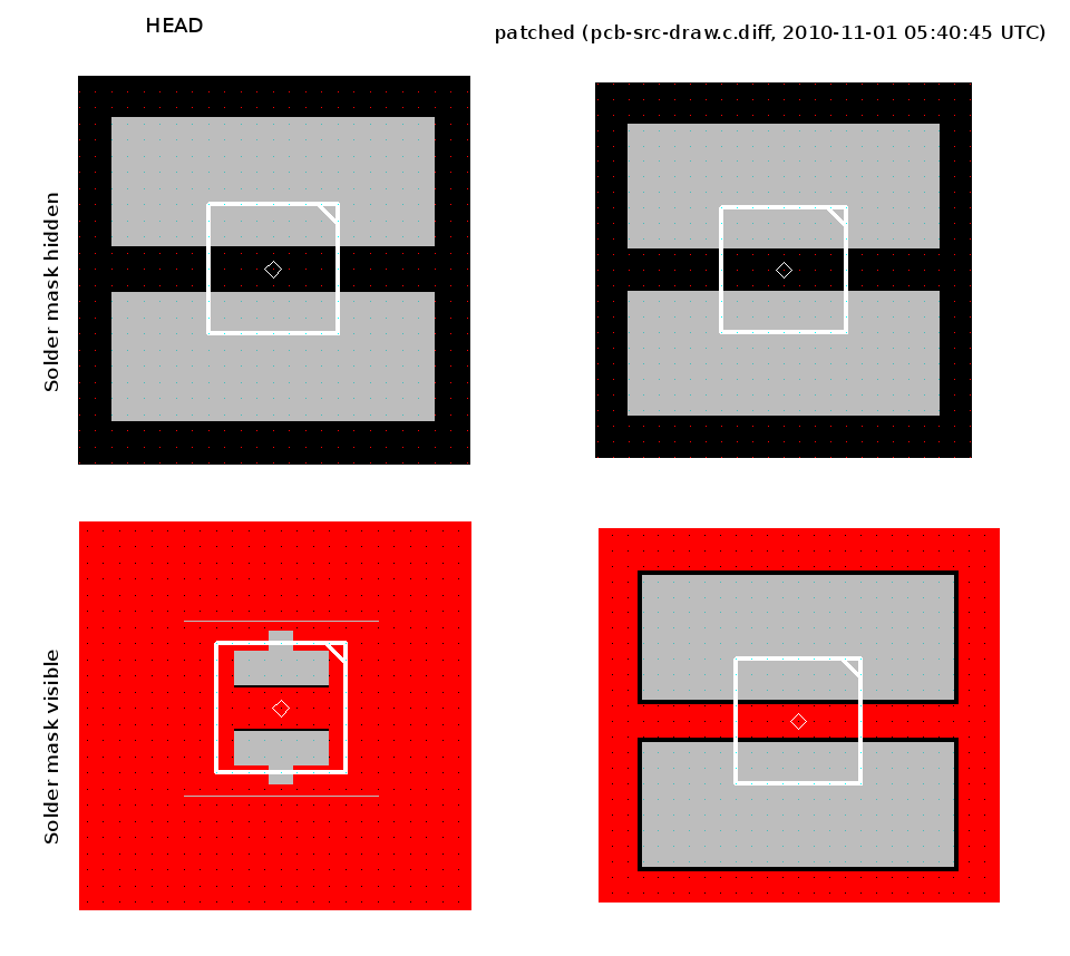
>
> > contact areas, presumably important to assist accurate placement of
> > the LED.
>
> Turns out resist is a better black-body emitter than shiny metals.
>
> > It looks like I can in fact set different solder mask clearances for
> > overlapping pads, but I have not been able to make a pad entirely
> > covered with solder mask.  Is this possible?  I found that
> > doing changeclearsize to 1 mil gave almost complete solder mask
> > coverage, but some copper was exposed.
>
> You should be able to set the mask to exactly zero, although it might
> be easier to edit the .fp file than do it in PCB itself.  You'll also
> need this bug fixed:
>
> https://sourceforge.net/tracker/?func=detail&aid=3100510&group_id=73743&atid=538813

Thanks for the footprint example. That is really helpful.
I built pcb HEAD with the patch (pcb-src-draw.c.diff dated 2010-11-01
05:40:45 UTC) from that bug applied and it seems worse.

With the patch applied, I actually get a much worse result with the
footprint example you provided.  The solder mask doesn't touch the big
pad at all.  See my screen shot collage at
<http://gibibit.com/upload/2010-11-10_pcb_mask_drawing1.png>.  The
lower-right image shows the patched version with the solder mask
showing.

> > Does anyone have any recommendations or tips for me on creating a
> > pcb footprint like the one on page 10 of the data sheet?
>
> Three pads per terminal.  One big one for the resist-covered parts,
> two overlapping small ones to make the T shape.  Something like this:
>
> Element["" "" "" "" 181102 181102 0 0 0 100 ""]
> (
>       Pad[-3543 4724 3543 4724 3937 1200 4537 "" "1" "square"]
>       Pad[0 7481 0 7874 2362 1200 2962 "" "1" "square,edge2"]
>       Pad[-11811 10630 11811 10630 15748 1200 0 "" "1" "square"]
>       Pad[-3544 -4725 3542 -4725 3937 1200 4537 "" "2" "square"]
>       Pad[0 -7874 0 -7481 2362 1200 2962 "" "2" "square"]
>       Pad[-11811 -10630 11811 -10630 15748 1200 0 "" "2" "square"]
>       ElementLine [-7874 -7874 7874 -7874 600]
>       ElementLine [7874 -7874 7874 7874 600]
>       ElementLine [7874 7874 -7874 7874 600]
>       ElementLine [-7874 7874 -7874 -7874 600]
>       ElementLine [5512 -7874 7874 -5512 600]
>
>       )

Thanks for taking the time to do this!

OT: Back in the 90's, when I was 13 years old and learning to program
using DJGPP, I would not have thought I'd be interacting with DJ
Delorie in 2010!  :-)  P.S. thanks for all your work on DJGPP in the
past as well as the gEDA project.

Regards,
Colin


_______________________________________________
geda-user mailing list
[email protected]
http://www.seul.org/cgi-bin/mailman/listinfo/geda-user