On Wed, Jan 20, 2016 at 02:13:35PM +0100, Richard Cochran wrote:
> On Wed, Jan 20, 2016 at 12:13:13PM +0100, Miroslav Lichvar wrote:
> > I would like to try this. I don't have an i210 card nearby, but I
> > assume it requires some soldering. Do you have any pictures that show
> > where the connection should go and how big is the pad?
>
> The card has a 6 pin header, so no soldering is required.  I couldn't
> find any documentation, and so I ohm'ed the pins out to the chip.
> I'll post a photo and my notes.
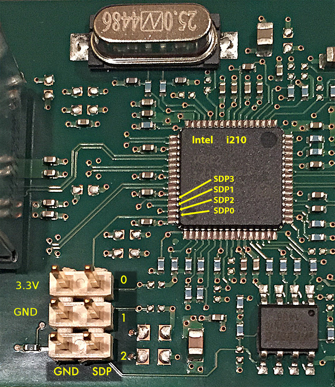
Rich Schmidt sent me this photo he had already made.

  http://linuxptp.sourceforge.net/i210/i210-SDPs.jpg

The "Software Defined Pins" (SDP) are on the right side of the 6 pin
header.  On the left side you have one 3.3V pin and two ground pins.

The signal level is CMOS, and there is no ESD protection at all.
Be careful!

The SDPs can be programmed as inputs (time stamps on signal edges) or
as outputs (periodic signals).  You can do some interesting things
with them.  I once made a BC with 3 cards on one mother board, letting
the "lead" card send a 1 PPS to the other two, using the external time
stamps to lock to the lead card.

HTH,
Richard

------------------------------------------------------------------------------
Site24x7 APM Insight: Get Deep Visibility into Application Performance
APM + Mobile APM + RUM: Monitor 3 App instances at just $35/Month
Monitor end-to-end web transactions and take corrective actions now
Troubleshoot faster and improve end-user experience. Signup Now!
http://pubads.g.doubleclick.net/gampad/clk?id=267308311&iu=/4140
_______________________________________________
Linuxptp-users mailing list
[email protected]
https://lists.sourceforge.net/lists/listinfo/linuxptp-users