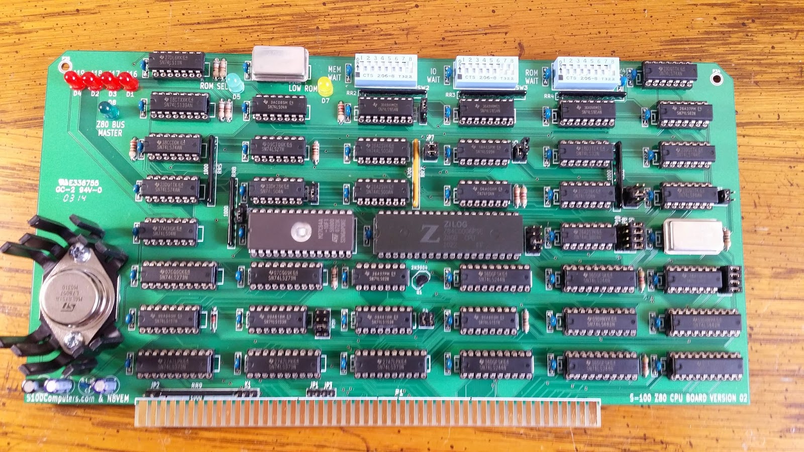
This is the board that I assembled.  I also have a couple of the boards
that Gary had made (with JP10)
but I haven't assembled them yet.
Ed

<https://lh6.googleusercontent.com/-9Mxy04RCORU/U-ZqTQt-u9I/AAAAAAAAAFk/daEJBGLom0k/s1600/20140809_133039.jpg>


On Saturday, August 9, 2014 1:24:53 PM UTC-5, monahanz wrote:
>
> Gary can you e-mail me your picture of the “V2a” board.  I seem to
> remember that was a second batch of the V2 board’s where we corrected the
> need for the 1K pull-up on the back, right?  I don’t have that one
>
> John
>
>
>
>
>
> *From:* [email protected] <javascript:> [mailto:
> [email protected] <javascript:>] *On Behalf Of *Gary Kaufman
> *Sent:* Saturday, August 9, 2014 11:14 AM
> *To:* [email protected] <javascript:>
> *Subject:* Re: [N8VEM-S100:4872] 2 different "Z80 CPU BOARD VERSION 02"
> pcbs out there
>
>
>
> Ed -
>
> The batch I had made up had the JP10 and K3 jumpers.  The jumper block
> diagram on John's site is the "earlier" version 02 board.    JP10 (not
> pictured) is above the LS04 just to the right of the top of the voltage
> regulator.  K3 is to the right of JP8.
>
> My jumper setting notes:
>
> (The * settings are the ones I used)
>
> I can email you a picture of the completed board if it would help.
>
> - Gary
>
> JP1    GND to OV_A (S100 pin 20) (normally open)
> JP2    GND to OV_B (S100 pin 53) (normally open)
> JP3    GND to OV_C (S100 pin 70) (normally open)
>
>
> JP4  *Reset to POC
> JP5    Reset from power
> JP6  *Reset to slave_clr
> JP7 * Reset from push button
>
> JP8    EPROM/EEPROM Pin 23 / A11
>     1-2    A11    *1-2 for 28C64 or 27C64
>     2-3    VCC
>
> JP9    EPROM/EEPROM Pin 26
>     1-2    VCC    *open for 28C64 or 27C64
>
> JP10    Onboard Rom
>         *Jumpered  Enabled
>         Open       Disabled
>
> K1      1-2    PWRFAIL to NMI        If NMI software is not implemented do
> not connect
>      2-3    NMI to NMI
>
> K2     1-2     older pre-IEEE696 boards
>     *2-3     clock disable of control lines
>
> K3    CPU Clock Source
>     *1-2     Oscillator
>      2-3    external CPU Clock (NDEF3)
>
> P2    Memory window configuration port
>     0xH to FxH
>         A4     1-2
>         A5     3-4
>         A6    *5-6        Output Ports D2H, D3H
>         A7     7-8
>
> P3    PROM Boot Address
>         A12
>         A13
>         A14
>         A15
>     *no jumpers    F000H
>
> P4    1-2    S-100 2Mhz clock signal to bus when z80 active
>     3-4    S-100 MWRT to bus when z80 active
>
> P8/P9/P10    Monitor Jump Location
>     P8      P9      P10
> 1    U15      GND      A15
> 2    U15     GND      A14
> 3    U15      GND      A15
> 4
>     *F000H    P8 1,2,3,4 to P10 1,2,3,4
>
>
> P36     Allows wait states
>      1-2  Every sINTA
>     *3-4  M1 memory bus cycles
>      5-6  All memory cycles
>
> P37    *1-2  Partial latch mode
>      3-4  Full latch mode
>
> P39  A12 Address Line to U13 (EPROM/EEPROM)
>
>      1-2  Tie to VCC
>      3-4  Tie to GND
>      5-6  Tie to A12
>     *7-8  Control by bit1 of port D3H
>
>     Output 00H to port D3H to select lower 4K of ROM
>     Output 01H to port D3H to totally remove ROM from the Z80's address
> space
>     Output 02H to port D3H to select upper 4K of ROM
>
> SW2    ME Wait states for P36 option
>     * switch 8 closed (right most) for 1 wait state, rest open
>
> SW3    I/O Wait states
>     * switch 7,8 closed (right most 2) for 2 wait state, rest open
>
> SW4    ROM Wait states for onboard EEPROM
>     * switch 8 closed (right most) for 1 wait state, rest open
>
>
>
> On 8/9/2014 1:54 PM, Edward Snider wrote:
>
> Hello all,
>
>
>
> I am in the process of trying to get my Z80 cpu card running, and I've
> noticed that
>
> there are definitely 2 different pcbs marked "Z80 CPU BOARD VERSION 02",
>
> I have them both in front of me.
>
>
>
> The one I built does not have a JP10 or K3 jumpers.  Is this actually a V1
> board then?
>
> I'm trying to figure out which schematics I should be looking at.
>
>
>
> Anyone know of any other differences, jumper settings, issues, etc, I
> should be aware of
>
> with this board?  So far I'm just trying to get the cpu into halt with an
> eprom full of 76's
>
> and not having any luck.  Probably don't understand the jumper settings
> well enough.
>
>
>
>
>
> Thanks,
>
>
>
> Ed
>
> --
> You received this message because you are subscribed to the Google Groups
> "N8VEM-S100" group.
> To unsubscribe from this group and stop receiving emails from it, send an
> email to [email protected] <javascript:>.
> For more options, visit https://groups.google.com/d/optout.
>
>
>
> --
> You received this message because you are subscribed to the Google Groups
> "N8VEM-S100" group.
> To unsubscribe from this group and stop receiving emails from it, send an
> email to [email protected] <javascript:>.
> For more options, visit https://groups.google.com/d/optout.
>

--
You received this message because you are subscribed to the Google Groups
"N8VEM-S100" group.
To unsubscribe from this group and stop receiving emails from it, send an email
to [email protected].
For more options, visit https://groups.google.com/d/optout.