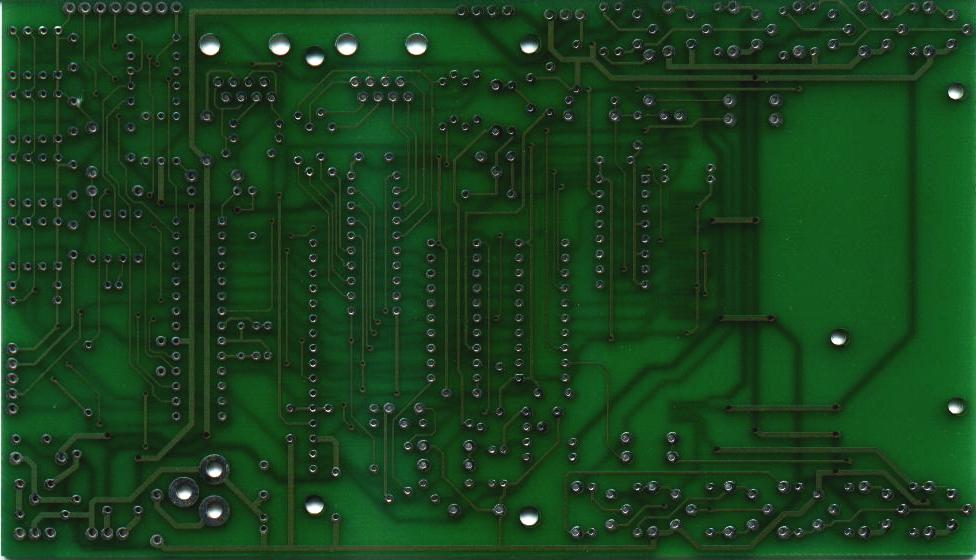
The boards arent 100% good because I dont use a very good film, so
it have a little distortion close the boards, and some drills are
not in the middle of the pin/via. Its just a prototype, so it is not
a problem to make sucha board with a cheapest photografric film.
I have some doubts to make the definitive board, it must be entirely
in SMD, and I dont know how to make visual targets, generate the glue
silk, coordinate files, and I dont know exactly it works, so, I have
to look closer about that...


On Wed, 23 Jul 2003 23:19:54 -0400
Dave McGuire <[EMAIL PROTECTED]> wrote:

> On Wednesday, July 23, 2003, at 06:38 PM, Xtian Xultz wrote:
> >  In the link below I put a image from a board I made with
> > gEDA and PCB only (and some programs like sketch, gv, etc).
> > The image is not good because it was made with a not-so-good
> > scanner, but is just an example.
> >
> > Any information you need I can help, just ask
> >
> > http://gpiclib.sourceforge.net/board1.jpg
> > http://gpiclib.sourceforge.net/board2.jpg
>
>    Nice looking boards!
>
>       -Dave
>
> --
> Dave McGuire                 "You don't have Vaseline in Canada?"
> St. Petersburg, FL                     -Bill Bradford
>
>