Thank you very much for your valuable feedback.
Just to make sure, this would be alright:
--------------------------------------
|       SMALLER PCB       |
--------------------------------------
   )¤¤¤(      )¤¤¤(      )¤¤¤(
----------------------------------------------
|          LARGER PCB              |
----------------------------------------------

the shorter PCB above the longer one connected by mouse bite tabs?

Oh, and since I will be ordering a stencil along with the PCBs, while
googling something related to it, I found this:
https://learn.adafruit.com/smt-manufacturing/laser-cut-stencils

The only thing I find interesting is where they suggest to make
modifications to the gerbers in order to shrink the size of the SMD pads:
"You'll
now see that your pads are thinner. This prevents bridging since the laser
is not perfectly precise and tends to 'go over' the boundaries by a few
mils."
Is it really needed? I have some QFN components with small pitch between
pads, I will be ordering the electropolished stencil for added precision.

Dana subota, 9. prosinca 2017. u 22:36:39 UTC+1, korisnik Allen Dutra
napisao je:
>
> Hi Luka,
>
> You are correct. Everyone that I've ever talked to, looks at that mess of
> board outlines you've circled and says "Mouse Bite". Ultimately any board
> outline is provided to a CNC technician and *interpreted *to create tool
> routing. Tool routing that is offset from the board outline by the drill
> radius and concave acute angles rounded. Often a good PCB Fabricator (fab
> shop) will point out areas that can't be CNC routed and work with the
> customer on a solution.
>
> Take way: board outlines and mouse bites are always interpreted by a
> technician to make sure the CNC routing works correctly. I've yet to see
> mouse bites done incorrectly though I've have seen the drill size, spacing,
> and count adjusted based on board thickness. If your building a thinner
> than standard boards a fab shop may adjust the mouse bite specification for
> reliability. Translation, make sure the mouse bite doesn't break in the
> factory but can be snapped latter by the customer.
>
> Done correctly you shouldn't need cutting tools to snap mouse bites.
>
> Allen
>
> On Sat, Dec 9, 2017 at 5:26 AM, Luka C <[email protected]
> <javascript:>> wrote:
>
>> @Allen I'm planning on assembling them "by hand", manually pick and place
>> SMD components and bake them inside a reflow oven. I guess I'll try
>> following the Dangerous Prototyping post today.
>> The only thing I do not understand is the part I've marked in yellow on
>> the picture here: https://i.imgur.com/HmpFPwv.jpg
>> Those break tabs contain outlines of both the first and the second board
>> as well as the arc. I suppose the technician at the fab house then alters
>> this in a way that the machine only cuts the arcs and not the board outline
>> directly around it as it would cut the two boards apart?
>>
>> @gregebert I'm was thinking about cutting them with something like that
>> indeed, I'd just like to make it easier by having empty space between them
>> and having mousebites to simplify cutting them apart.
>>
>> Dana subota, 9. prosinca 2017. u 04:17:25 UTC+1, korisnik Allen Dutra
>> napisao je:
>>>
>>> Hi Luka,
>>>
>>> Allen Dutra, professional PCB designer currently working for Apple and
>>> with a lot of first hand experience with PCB panels.
>>>
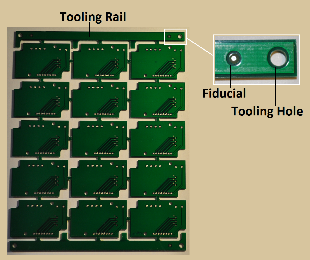
>>> In your case you want to use mouse bites to combine two different sized
>>> rectangles. V-Scores won't work here. The mouse bite instructions from
>>> dangerous prototypes will work well for standard 0.064" designs. Question,
>>> are you soldering these boards by hand or having them built on an assembly
>>> line? (I could guess your answer but no assumptions from me) Assembly lines
>>> will want tooling rails
>>> <https://www.pcbuniverse.com/articles/Tooling%20Rails,%20Holes%20and%20Fiducials.png>
>>>
>>> for best results but these are easily forgotten.
>>>
>>> I haven't use the PCB Panelizer tool that you linked to. Generally I
>>> design my panel in the ECAD tool (Eagle CAD, Allegro, Altium etc.) I'm
>>> already using to ensure Gerber accuracy.
>>>
>>> Let me know if you have other questions,
>>>
>>> Allen
>>>
>>> On Friday, December 8, 2017 at 5:07:06 PM UTC-8, Luka C wrote:
>>>
>> --
>> You received this message because you are subscribed to a topic in the
>> Google Groups "neonixie-l" group.
>> To unsubscribe from this topic, visit
>> https://groups.google.com/d/topic/neonixie-l/Y0gwQHuCzoE/unsubscribe.
>> To unsubscribe from this group and all its topics, send an email to
>> [email protected] <javascript:>.
>> To post to this group, send email to [email protected]
>> <javascript:>.
>> To view this discussion on the web, visit
>> https://groups.google.com/d/msgid/neonixie-l/67036d33-d5a0-465e-8f20-57f96a9acbe2%40googlegroups.com
>>
>> <https://groups.google.com/d/msgid/neonixie-l/67036d33-d5a0-465e-8f20-57f96a9acbe2%40googlegroups.com?utm_medium=email&utm_source=footer>
>> .
>>
>> For more options, visit https://groups.google.com/d/optout.
>>
>
>

--
You received this message because you are subscribed to the Google Groups
"neonixie-l" group.
To unsubscribe from this group and stop receiving emails from it, send an email
to [email protected].
To post to this group, send an email to [email protected].
To view this discussion on the web, visit
https://groups.google.com/d/msgid/neonixie-l/7c5b6249-6105-408e-8fc6-c7fbb7af9226%40googlegroups.com.
For more options, visit https://groups.google.com/d/optout.