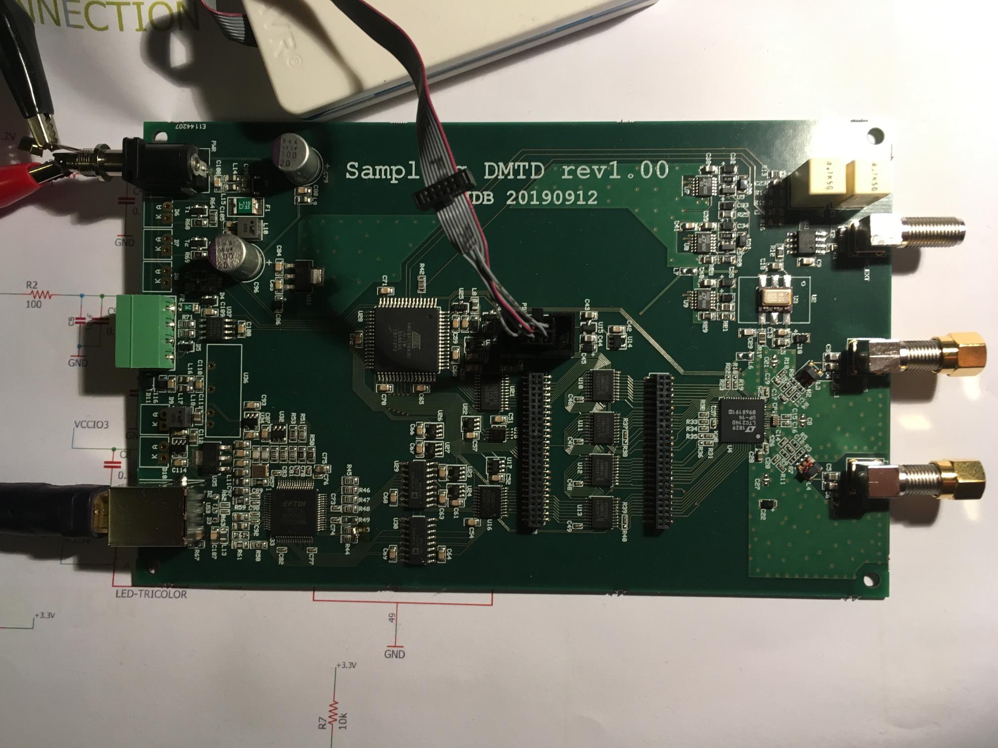
Update: last Friday our students have populated a few prototype boards (
http://www.lartmaker.nl/time-nuts/dmtd-proto.jpg), and this weekend I
managed to get some early code running on it.
The good: Noise performance matches the datasheet (1.19LSB_RMS given,
1.21LSB_RMS measured). The 1/f corner is much lower than I feared (
http://www.lartmaker.nl/time-nuts/LTC2140-14%20noise%20corner.pdf ;
measured at a sample rate of 10ksps with terminated inputs, PSD averaged
over 500M samples in 1Msample chunks with a rectangular window), and direct
measurements at a 10Hz beat frequency should be possible. (I don't
completely trust this data yet; the absence of 50Hz lines in an unshielded
setup makes me suspicious.)

The bad: LF noise / drift is significant (
http://www.lartmaker.nl/time-nuts/LTC2140-14%20drift.pdf; vertical axis is
in LSB). On a 0dBFS signal with a 10Hz beat note an uncertainty of 0.25LSB
in the zero crossing point would translate to +/-1ps; what I'm seeing here
would eat my entire error budget and then some. I need to find a
computationally cheap way to filter this, or move to the FPGA after all.

The ugly: I can't get the FT2232H channel A to work in asynchronous
FIFO-mode. I have programmed the EEPROM wth the latest version of the
FT_PROG tool, but the TXE# line stays high (under Linux; I'm reading data
from /dev/ttyUSBx with ftdi_sio, a setup which FTDI hints should work). I
haven't looked too hard yet as I have the serial port as a backup, but it
would be nice to get this working.

To be continued,

JDB.
[listadmin: do let me know if you feel these updates are more noise than
signal]

On Sat, Sep 14, 2019 at 2:25 PM Jan-Derk Bakker <jdbak...@gmail.com> wrote:

> Update: I have finished routing the board (placement diagram at
> http://www.lartmaker.nl/time-nuts/DMTD%20rev1.00%20assembly.pdf ) and
> ordered a few prototype PCBs.
>
> After the earlier discussions on the list I've grown sufficiently
> concerned about the impact of 1/f converter noise that I have added headers
> to the board to allow me to replace the D-flipflop sampler with an
> FPGA-based I/Q downconverter. While the main PCBs are in production I'll
> draw a simple daughterboard with dual ice40 UltraPlus FPGAs, If the FPGA
> solution turns out to be necessary (or a noticeable improvement), I'll
> redraw the main PCB.
>
> To be continued,
>
> JDB.
>
> On Sun, Sep 1, 2019 at 2:09 AM Jan-Derk Bakker <jdbak...@gmail.com> wrote:
>
>> Dear all,
>>
>> I've been working on a design for a (relatively) simple, standalone
>> sampling DMTD. Very rough preliminary schematics can be found at
>> http://www.lartmaker.nl/time-nuts/DMTD_rev0.99.pdf .
>>
>> Design goals are:
>> - ps-level accuracy
>> - comparison of frequencies between at least 10 and 50MHz, preferably
>> between 1 and 100MHz
>> - comparison of (selected) different frequencies (in my case: 10MHz vs
>> 50MHz)
>> - standalone operation, field-portable
>> - option for raw data sampling / (post)processing on a PC
>> - option for generating a tuning voltage to lock the measured oscillator
>> to the reference, so the DMTD can act as a PLL in phase noise test setups
>>
>> Context: you may remember that a year or two ago I posted to time-nuts
>> about a GPSDO-design geared for mobile applications, which I was working on
>> for an SDR-platform my students are working with. This SDR-platform has now
>> grown to include a 100-channel phased array receiver. To validate the
>> reference clock distribution in this array (amongst other things) I would
>> like to have a DMTD. As the commercial offerings are outside the budget of
>> our lab, I was planning to roll my own.
>>
>> The core of the system is a transformer-coupled LTC2140-14 dual 14-bit
>> ADC, sampling at an offset frequency of nominally 10MHz+10Hz generated by a
>> VCTCXO (with an option for an OCXO). The ADC was chosen for its large input
>> bandwidth and small aperture jitter. Simulations of a simple software ZCD
>> consisting of a digital filter and least-squares fitting showed that
>> 100ksps would be more than enough to get the desired accuracy. As the ADC
>> design is unable to achieve sample rates lower than 1MSPS, D-flipflops are
>> used to decimate the samples. These DFFs are also used to multiplex the
>> 2x14-bit samples to an 8-bit data bus going into one of the GPIO-ports of
>> an XMega. The XMega runs the ZCD, and generates a tuning voltage for the
>> offset oscillator. Communication to a logging PC is done with a
>> galvanically isolated FT2232H, which has both an ASCII COM-port for the ZCD
>> data and a control interface and an asynchronous FIFO to transfer raw
>> samples. System power comes from the isolated USB bus or a barrel jack; BOM
>> cost in qty10+ is around 100US$.
>>
>> (The DMTD has a few more power rails than I would have liked. Originally
>> I had planned to use the LTC2295 and have a 3v3-only system, but after
>> re-reading the NIST paper on SDR-as-a-DMTD I concluded that the single
>> clocking path of the 2140 would likely have better aperture jitter
>> correlation between the channels. As a 1.8V/10MHz XMega would only be
>> borderline able to handle the computations, I ended up with this design.
>> LVC logic is used to go from 3.3V->1.8V, LV1T translators for the opposite
>> direction.)
>>
>> Design decisions and/or non-goals:
>> - I considered putting a small FPGA (specifically a Lattice ice40
>> UltraPlus) between the ADC and the processor. This was rejected because the
>> performance of the decimator appeared to be sufficient, and I wasn't
>> certain that I could get DDR mode + a CORDIC working in this FPGA.
>> - Especially when I found the necessity to move part of the system to
>> 1.8V I considered moving to an ARM. I stuck with the XMega as performance
>> was sufficient, and I am very familiar with both the CPU and the
>> peripherals (particularly time-stamping counters and the Event system) that
>> would ease the ZCD implementation and issues like synchronization between
>> processor and sampling system.
>> - I looked into integrating a phase noise measurement, but could find no
>> easy way that wouldn't degrade DMTD operation in the process. The tuning
>> voltage output is an inexpensive compromise (as I still had a DAC and
>> enough cycles to spare)
>> - The main thing I'm unsure about is the effect of the balun on phase
>> performance wrt temperature and termination matching. I've kept to the
>> baluns as they add less noise than a fully differential amplifier would.
>>
>> While I've made this design for my own purposes, I would be more than
>> happy to put it under an Open Hardware-license and/or work with TAPR or
>> other parties to get it distributed, should there be interest.
>>
>> Thoughts?
>>
>> with kind regards,
>>
>> Jan-Derk Bakker
>> [planning to start board layout tomorrow; looks like this should
>> definitely fit on a 100x160mm Eurocard inside a Hammond 1455-series box]
>>
>
_______________________________________________
time-nuts mailing list -- time-nuts@lists.febo.com
To unsubscribe, go to
http://lists.febo.com/mailman/listinfo/time-nuts_lists.febo.com
and follow the instructions there.