Hi Vasile,

I've committed my last try, including aeras with GND signals, propagated
over the board (I've finally managed to use polygons with rastness option).
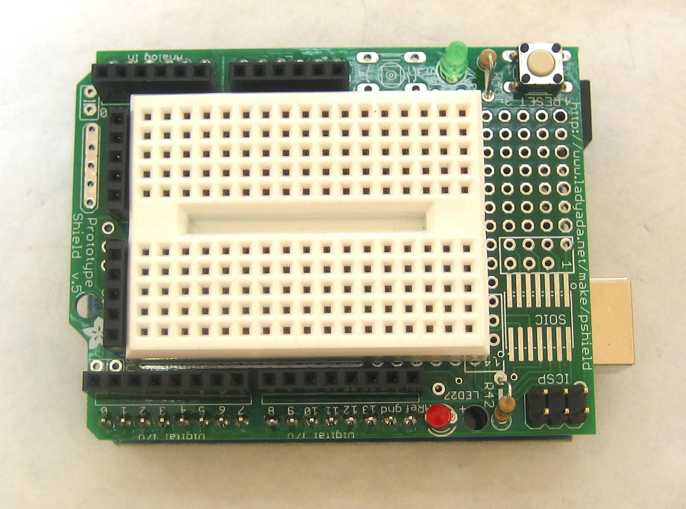
> Unconected shield areas acts as antennas for the adjacent signals near the
> area.
> I think the GND should be also connected to some connectos.
>

GND is currently connected to 3 pins, 2 pins adjacent, and 1 on another
connector. I can't decide where to put GND on pins, this is imposed by
either Jaluino pins or Arduino pins.


> For a goos shield  design at home, use a double layer PCB, design routes on
>  one layer and keep the other layer as ground isolating the component pins
> with a large drill in the copper (ie, a 0.8 drill diameter, 1.5 or 2mm
> diameter for copper isolation). This tehnique is used to produce high
> quality RF PCB's at home.
>
Connect with more vias (at least 10-20 for DC or PICmicro design and up to
> thousens for RF - not suitable for home) between the ground planes of the
> layers.
> Try to go smaller as possible with your PCB designs, keeping an easy way to
> replace any components. This is the right way for increasing PCB design
> performance.
>
>
I can't produce a double layer PCB at home... More, as I said, these shields
aren't RF shields, but "just" daughter boards. In any case, I clearly won't
fell confortable when it come the time to design advanced high quality RF
PCBs... :)

I'll try to build the current one, as a Proof Of Concept. It'll mainly be
used to plug prototype board, like this one:
http://www.ladyada.net/images/pshield/miniproto.jpg . As for other more
advanced Arduino shield, we'll have to check... or design our own.


Cheers,
Seb
--
Sébastien Lelong
http://www.sirloon.net
http://sirbot.org


>
> On 9/10/09, Sebastien Lelong <[email protected]> wrote:
>>
>> This one might be better, there's no bridge except two for connecting
>> large areas of GND signals (I don't know if this is much useful...)
>>
>> Seb
>> --
>> Sébastien Lelong
>> http://www.sirloon.net
>> http://sirbot.org
>>
>>
>> 2009/9/10 vasile surducan <[email protected]>
>>
>>> Hi Seb,
>>>
>>> I am appreciating your enthusiasm, however the shield you've designed it
>>> hasn't too much ability of shielding.
>>>
>>> If your need carrying PWM signals from one board to other, where both or
>>> only one board has also analogic areas, you must be very carefull. You need
>>> two layers and ground planes on both layers connected through a number of
>>> vias.
>>>
>>> If your application is pure digital, both boards without any analogic
>>> area, then shielding is not important.
>>>
>>> If the PWM is used for generating a clean analogic signal after a
>>> filter, could be a serious problem (clean PWM filtering with first order
>>> filters is impossible, no matter what you have seen on the enthusiastics
>>> websites; clean means lower than 5mV ripple).
>>>
>>> Learn to avoid in your design 90 degree direction changes in your routes
>>> as a general rule. If you have two layers, use traces equaly on both
>>> layers. Avoid multiple layer changes on clocks, PWMs and other agressing
>>> signals. Designing a PCB it's like programming. You can't do it well if you
>>> don't do it continously...Biggest problems start on 8-12 layers, but two
>>> layers an a PIC it's a good start.
>>>
>>>
>>>   On 9/10/09, Sebastien Lelong <[email protected]> wrote:
>>>
>>>>  Hi guys,
>>>>
>>>>
>>>> I've committed Jaluino PCB & schematic template for Eagle (see
>>>> http://code.google.com/p/jallib/source/browse/trunk/project/jaluino/schematics/jaluino_shield_template_eagle.zip).
>>>> From this, I tried to create a shield that could act as a layer, an
>>>> intermediate, between Jaluino shields and Arduino shields. The idea is to
>>>> plug this intermediate shield onto Jaluino board, then plug an original
>>>> Arduino shield on top of this.
>>>>
>>>> Attached are pictures of:
>>>>
>>>>   - schematic: with mapping between Jaluino & Arduino pins. For PWM
>>>> channels, one is taken from RC2/CCP1, another is taken either from RC1/CCP2
>>>> or RB3/CCP2. RC1 and RB3 are multiplexed, so you can choose which of these
>>>> two pins will carry PWM. Using this approach, it may increase compatibility
>>>> (still only 2 PWM channels will be available, but for one, you can choose
>>>> where). As for analog pins, RA3/AN3 is mapped with AREF. Other mappings are
>>>> quite explicit. I'm open to suggestions !
>>>>
>>>>   - PCB: the resulting PCB. Green aeras are considered as blue tracks
>>>> (but couldn't make them blue...). Quite a lot of vias, not that beautiful,
>>>> sorry...
>>>>
>>>>
>>>> Finally, I had a hard brainstorming (not just with myself this time), to
>>>> find a name for this shield: "Styx". So this is Jaluino "Styx" shield. Why
>>>> ?
>>>> Well... Well in Greek Mythology, Styx is the river between Earth and
>>>> Underworld, a clear frontier between two worlds. I hope this illustrates as
>>>> good as possible the main purpose of this shield. Defining which part is
>>>> Earth, which part is Underworld in our case is left to readers' objectivity
>>>> :)
>>>>
>>>>
>>>> http://en.wikipedia.org/wiki/Styx for more...
>>>>
>>>>
>>>> [image: Dor%C3%A9_-_Styx.jpg]
>>>>
>>>>
>>>>
>>>> Cheers,
>>>> Seb
>>>> --
>>>> Sébastien Lelong
>>>> http://www.sirloon.net
>>>> http://sirbot.org
>>>>
>>>>
>>>>
>> >>
>>

--~--~---------~--~----~------------~-------~--~----~
You received this message because you are subscribed to the Google Groups
"jallib" group.
To post to this group, send email to [email protected]
To unsubscribe from this group, send email to
[email protected]
For more options, visit this group at
http://groups.google.com/group/jallib?hl=en
-~----------~----~----~----~------~----~------~--~---
<<attachment: jaluino_shield_styx_pcb.png>>