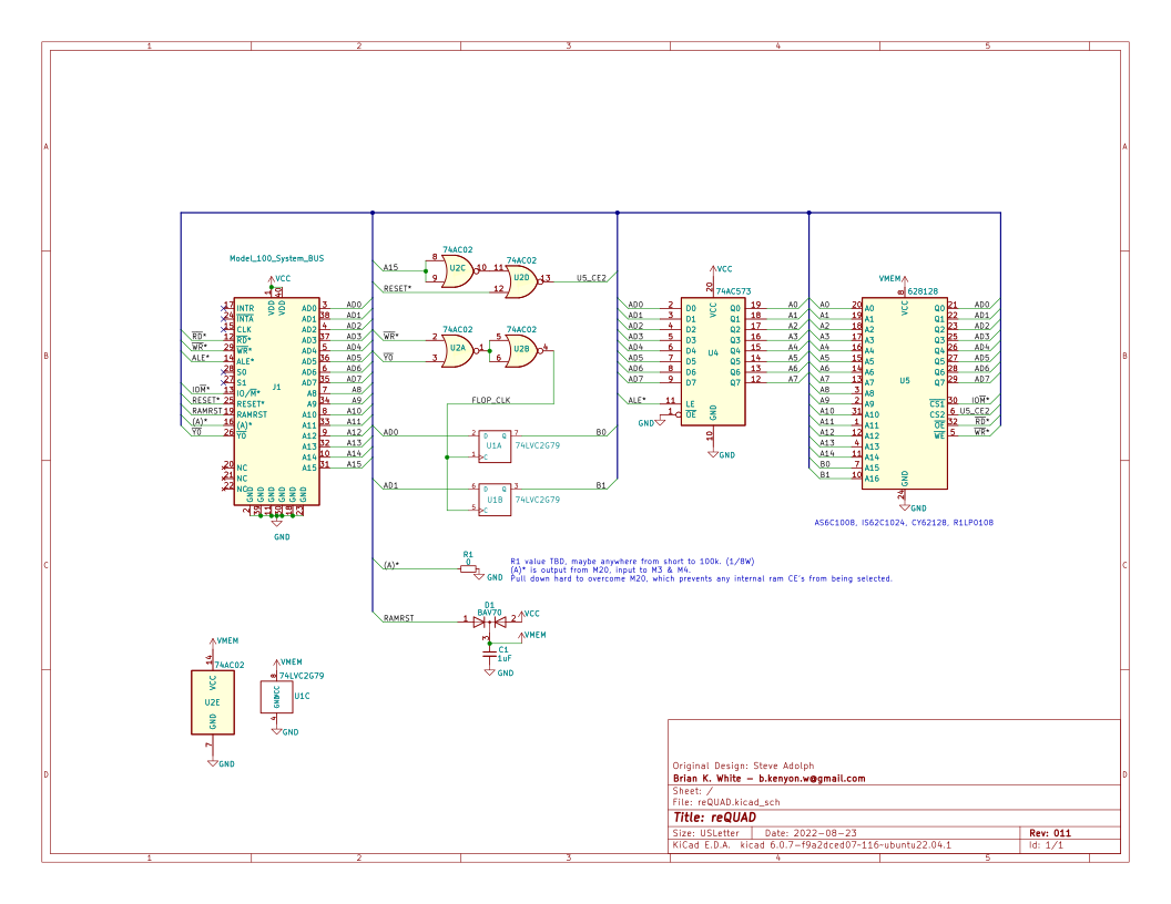
Heads up though, Steve has me convinced about that (A)* idea he
mentioned in an earlier post.
I've made a new version based on that idea but it needs some testing to
work out how hard (A)* should be pulled, a dead short or a resistor of
what value? A simple short would make the pcb simpler but right now I
made room and got an 0805 footprint crammed in there.
I'm going to rig up a test using one of my older version boards that I
already have without needing to wait for it to be made. My latest
versions were just like this with the only difference being (A)* is N/C.
That's convenient because it's trivial, all that needs is a single bodge
wire from bus pin 16 to gnd, maybe through a resistor.
The idea is, original QUADv4 disables the internal ram by holding RAMRST
high, which ends up blocking /OE on all the internal ram.
The new idea is leave RAMRST alone (other than using it for power, but
don't override it), instead, hold (A)* low. This blocks the (A)* signal
output from M20 reaching M3 & M4 input, which prevents any /CE1-/CE16
from being selected.
So rather than having all the internal ram active but just output
disabled, the ram is all inactive.
It's still overriding something, it just goes from overriding RAMRST to
overriding (A)*. (A)* is an output from M20, and I don't know what it
means for M20 to just short an output to gnd, but Steve already said he
tested it and it seems fine, and other commercial products even
supposedly did that.
What I want to do is see if maybe a resistor can pull it down good
enough to inhibit M3 & M4 from activating, and see just what it takes.
Maybe the output is pretty strong and maybe it takes a pretty low value
resistor to overcome it, but maybe anything is better than nothing and
maybe we can at least reduce the current through that output a little.
Or maybe a simple trace is no problem after all. Either way I want to
try it to find out.
This version is in the v011 branch until it's tested.

https://raw.githubusercontent.com/bkw777/reQUAD/v011/PCB/reQUAD.svg
https://github.com/bkw777/reQUAD/tree/v011
The pcb is done too, and the bom is good except it's missing the
resistor. But no links to buy a pcb because this isn't verified yet.
That's not a bad idea about the on-board battery. The PG Design version
of this has an on-board battery, but it's a bit more complex device and
works somewhat differently since it does not conflict with the internal
ram. The internal ram becomes bank1, and the added ram is banks 2
through 8 depending on what size model. It's pretty handy that you can
remove the device and not lose the contents.
http://tandy.wiki/PG_Design
https://photos.app.goo.gl/m8rpRFAL22FcjxLu6
That device looks a bit more complicated though to allow not fighting
with the internal ram, and have a battery without draining it
immediately. For one thing, most of it's logic is actually all in a PAL.
(the chip with the barcode sticker on it in the pics there)
A similar device from Cryptronics also had a battery, a larger 3-cell
pack connected by wires, soldered, and stuffed in between the optrom &
bus socket.
https://photos.app.goo.gl/68qSfxdPD9WwdhzHA
Looks like a user bodge, but I've seen other pictures and they
apparently all shipped this way. I have one but have never fired it up,
so I don't know if it blocks out the internal ram or not. That thing has
a lot going on "the hard way" with no PAL.
The silkscreen says 64K, but there *appears* to be 96K worth of chips.
There are 12 chips, but they are stacked and you can only see the
markings on the top set, which is 4 x 6264, which is 4 x 8KB for 32K.
It's possible the hidden chips are not 6264, or possible the unit is a
revision that stuffs more ram onto the same pcb.
Those chips on the bottom of the pcb are actually installed upside down
from the point of view of the pcb surface, but it's so they can be in
same orientation as the rest of the stack. That's why you can't read any
markings. Notice the injection mold marks. The entire stack of 3 chips
must all be connected parallel right through the board except for a
couple control lines. They must have had to bend all those pins with a jig.
Lot of hand work on that puppy.

--
bkw


On 8/23/22 22:52, Henner Zeller wrote:
Thanks both Stephen and Brian for working on QUAD and Brian for the dive
into the history and sharing some of the gotchas discovered.
I think this last version looks very nice
* we have power all the time, using the VDD or RAMRST signal as power
source
* Due the diodes, we get to use the RAMRST as power source, but also
allow to backfeed
* the flip-flops retain their state, as they are powered by the same
VMEM, so everything
should be preserved on reset/power-cycle
* There is even a free diode on Pin 4 of the BAV04 one could connect
a local CR2032 backup battery
      (... if it can be made fit on the board)

I like it.
I have a 128kx8 (LP621024) in my project drawer, I think I'll start
building one of these to get some experience in seeing how I can use
bank-switching when writing software for the M100.
(different footprint, so I'll have to spin a new board; will send a
pull request),
Thanks,
   Henner.
On Tue, 23 Aug 2022 at 13:39, Brian K. White <[email protected]
<mailto:[email protected]>> wrote:
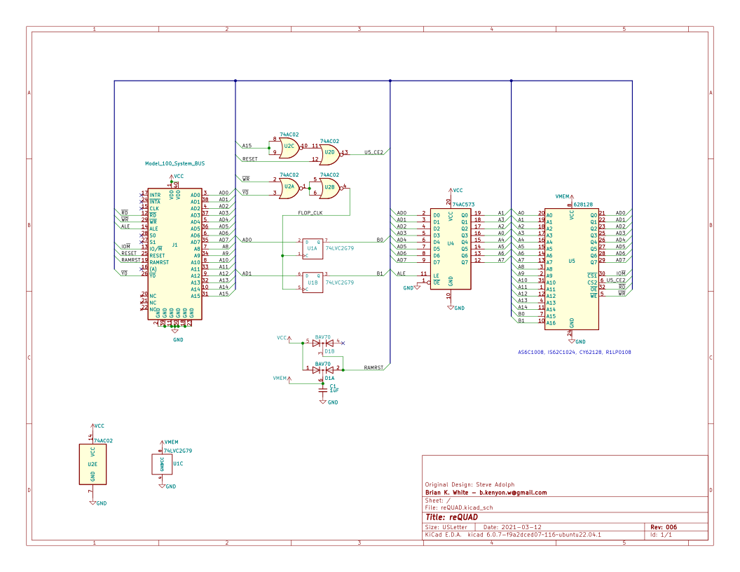
    Updated. The main branch is now essentially v006 which adds back in a
    diode I'd removed which backfeeds ramrst when vcc has power (to keep
    the
    internal ram disabled), plus switched U2 to power from vmem, so now all
    logic and ram are powered from vmem together, and same as before
    removes
    the resistor-cap power-on-reset.
    https://raw.githubusercontent.com/bkw777/reQUAD/main/PCB/reQUAD.svg
    <https://raw.githubusercontent.com/bkw777/reQUAD/main/PCB/reQUAD.svg>

    What was main below is now branch v008.
--
bkw
    On 8/23/22 04:10, Brian K. White wrote:
     > Steve raised a couple questions about my changes to QUAD that I
    don't
     > have good answers for, so I added all my previous versions into that
     > github repo as branches named v001, v002 etc, because at least a few
     > of those DO work, especially the early versions before I got all
    hack
     > happy.
     >
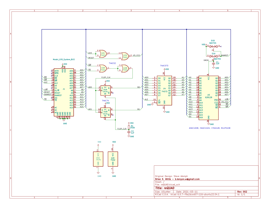
     > v002 is the version that exactly matches the QUADv2 schematic on
     > bitchin100
     > https://github.com/bkw777/reQUAD/tree/v002
    <https://github.com/bkw777/reQUAD/tree/v002>
     >
     > I think I must have gotten my versions 1 & 2 files mixed up.
     >
     > Looking at the different schematics, it looks like the
    progression goes:
     >
     > v002 -initial - identical schematic to QUADv4 original (new pcb
    layout
     > though)
     >
    https://raw.githubusercontent.com/bkw777/reQUAD/v002/PCB/reQUAD.svg
    <https://raw.githubusercontent.com/bkw777/reQUAD/v002/PCB/reQUAD.svg>
     > For comparison:
     > http://bitchin100.com/wiki/images/7/7b/QUAD_schemactic.png
    <http://bitchin100.com/wiki/images/7/7b/QUAD_schemactic.png>
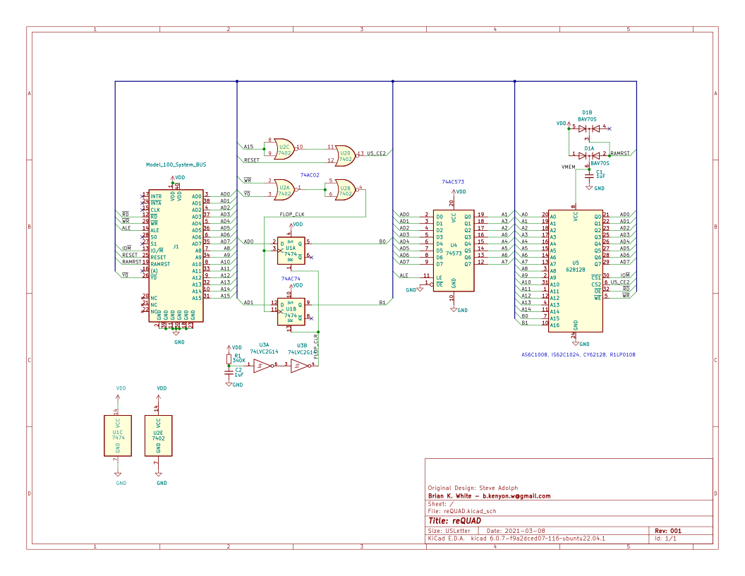
     >
     > v001 - add schmidt triggers to power-on-reset output (I think
    this is
     > an idea Steve might have suggested to me to try)
     >
    https://raw.githubusercontent.com/bkw777/reQUAD/v001/PCB/reQUAD.svg
    <https://raw.githubusercontent.com/bkw777/reQUAD/v001/PCB/reQUAD.svg>
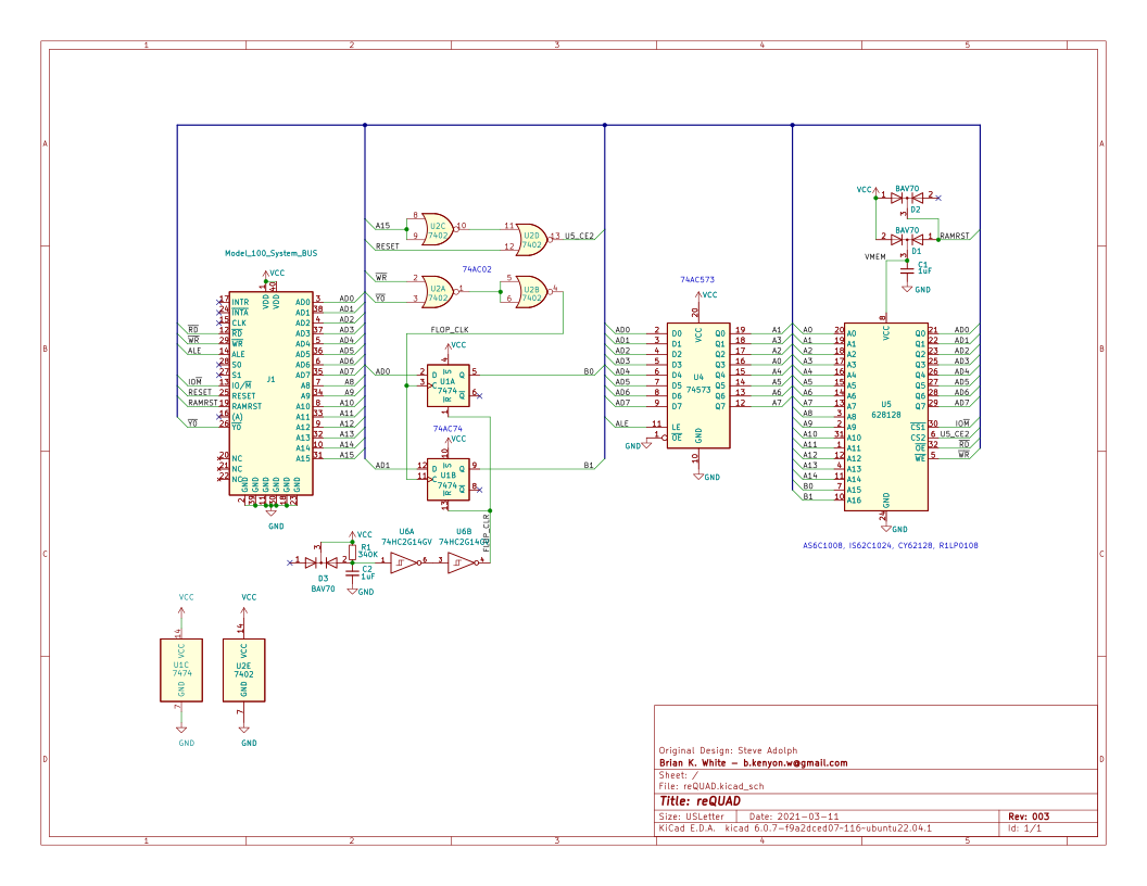
     >
     > v003 - add a diode across the p-o-r resistor (I might have got this
     > from reading about r/c p-o-r circuits in general)
     >
    https://raw.githubusercontent.com/bkw777/reQUAD/v003/PCB/reQUAD.svg
    <https://raw.githubusercontent.com/bkw777/reQUAD/v003/PCB/reQUAD.svg>
     >
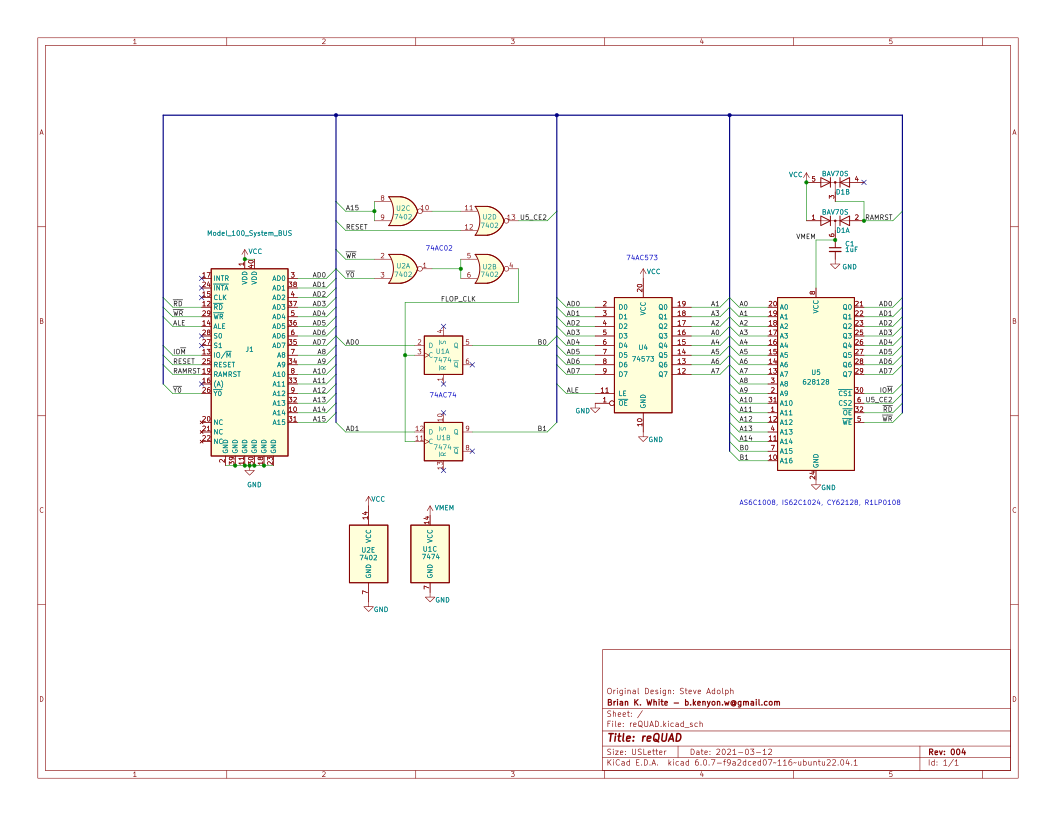
     > v004 - junk
     >
    https://raw.githubusercontent.com/bkw777/reQUAD/v004/PCB/reQUAD.svg
    <https://raw.githubusercontent.com/bkw777/reQUAD/v004/PCB/reQUAD.svg>
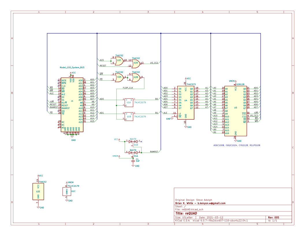
     >
     > v005 - remove p-o-r, switch to a non-resettable flipflop, power
     > flipflop from vmem (fail to power u2 from vmem)
     >
    https://raw.githubusercontent.com/bkw777/reQUAD/v005/PCB/reQUAD.svg
    <https://raw.githubusercontent.com/bkw777/reQUAD/v005/PCB/reQUAD.svg>
     >
     > v006 - same schematic as v005, pcb layout changes only (pull the
    chips
     > in from the ends so that a chip-puller doesn't hurt anything)
     >
    https://raw.githubusercontent.com/bkw777/reQUAD/v006/PCB/reQUAD.svg
    <https://raw.githubusercontent.com/bkw777/reQUAD/v006/PCB/reQUAD.svg>
     >
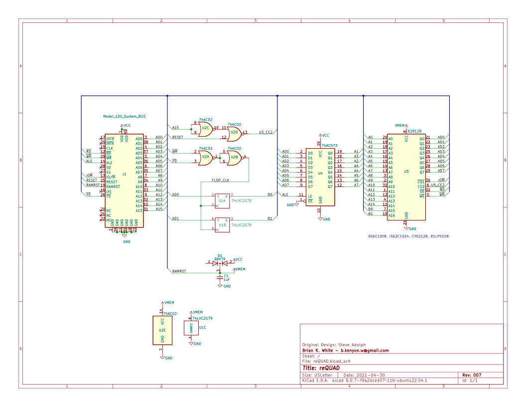
     > v007 - junk (but one correct change: move U2 to vmem)
     >
    https://raw.githubusercontent.com/bkw777/reQUAD/v007/PCB/reQUAD.svg
    <https://raw.githubusercontent.com/bkw777/reQUAD/v007/PCB/reQUAD.svg>
     >
     > main - junk - move ramrst, unshuffle the address lines output
    from U4
     > so that Q0 -> A0 Q1->A1 etc no idea if that was ok, I intended to
    test
     >
    https://raw.githubusercontent.com/bkw777/reQUAD/main/PCB/reQUAD.svg
    <https://raw.githubusercontent.com/bkw777/reQUAD/main/PCB/reQUAD.svg>
     >
     > So I think what we want is v006 but change U2 to get power from vmem.
     > Or one of v001,2,3 I'm not sure which is best, but any of 1-3 is
     > probably safe and more or less the same as the original.
     >
     >
     > At least a few of those versions do work, or at least appear to.
    I did
     > build a few and run them, but my testing was only cursory.
     >
     > I think until further notice, consider this stuff food for
    discussion
     > only, not claimed to be good, especially the last version.
     >
--
bkw
--
bkw