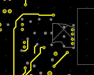
On Dec 22, 2017, at 20:38, Luke Kenneth Casson Leighton <[email protected]> wrote:
> On Fri, Dec 22, 2017 at 10:32 PM, Richard Wilbur
> <[email protected]> wrote:
>> Here's another view of the connector end with some slight revisions of
>> the ground fill and keepout boundaries between the ESD and connector
>> components.
>>
>> Summary:
>>
>> 1.  I moved the East extent of the layer 3 ground fill east to the
>> edge of the connector pads.
>
> ok remember that ground flood-fill is the entire layer 3, i'm not
> creating a *specific* area for ground "fill", it's done by default
> according to the (specified) design rules.  with the new "conditional"
> rule added, layer 3 now looks like this:
> http://hands.com/~lkcl/eoma/a20/275_hdmi/layer3.jpg
>
> so there's a few things i need to sort out, which i'll get to: main
> reason for showing that image is: the clearance to the VIAs has also
> extended to 15mil now.  i believe it's not so much the vias though as
> the tracks connected *to* the vias.  if there has to be a 5 mil
> clearance to those i can... maybe sort something out :)
15mil clearance to HDMI nets and vias won't hurt anybody's feelings!  Looks
good (minus the keepout under the connector).

[…]

>> 3.  The layer 2,3,4 ground keepout West edge moved with the East edge
>> of the layer 3 ground fill to the edge of the connector pads.
>
> oh wait... i haven't put in a keepout *at all* on layers 3 and 4.
> you think it would be best to punch the hole *right* down so that it's
> only layer 5 providing a GND plane for both sides?  it makes sense, i
> just want to confirm.

Yes, that is what I was asking for under the high-frequency differential
signals at the connector.  If you have reservations about it, let me know.  I'm
happy to get feedback from another perspective.


_______________________________________________
arm-netbook mailing list [email protected]
http://lists.phcomp.co.uk/mailman/listinfo/arm-netbook
Send large attachments to [email protected]