Hi Dominique,

Are you using a standard DMM to make your resistance measurements? If not,
you may have more consistent results by using a laboratory DMM that is
rated to measure milliohms.
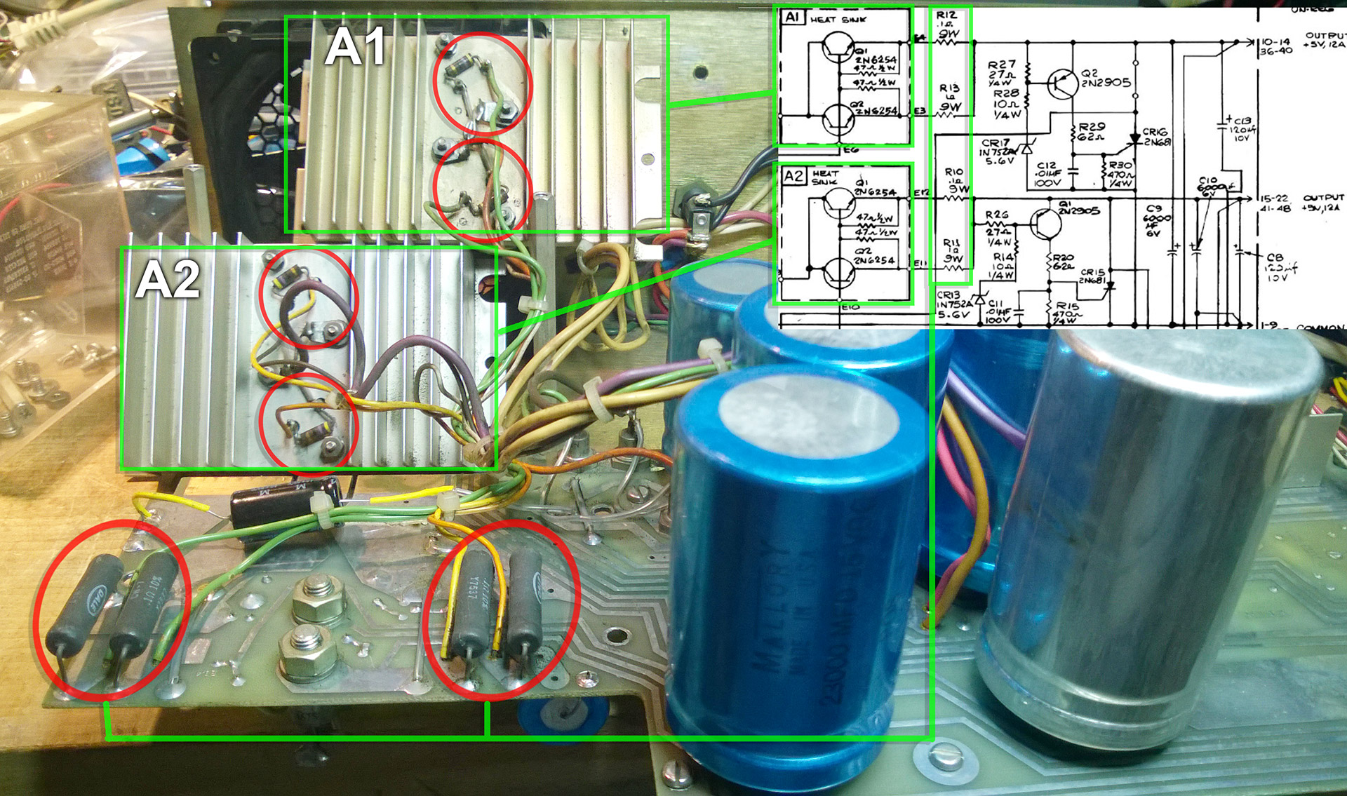
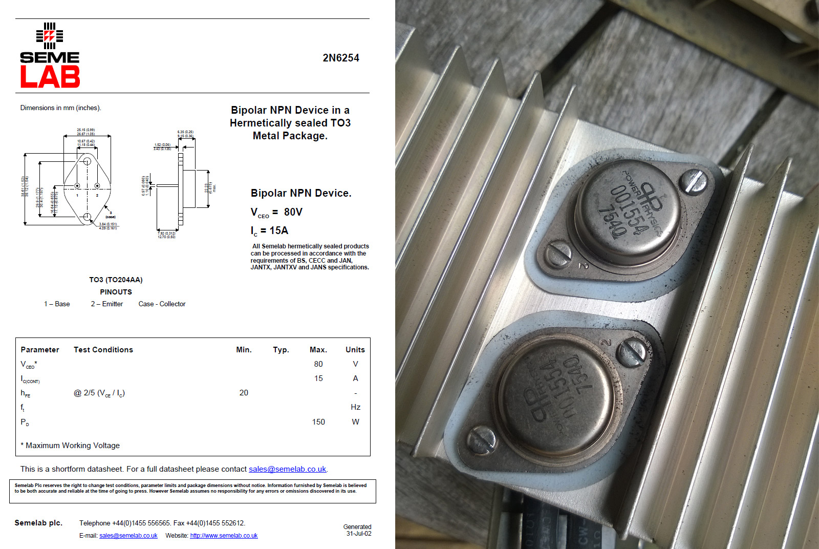
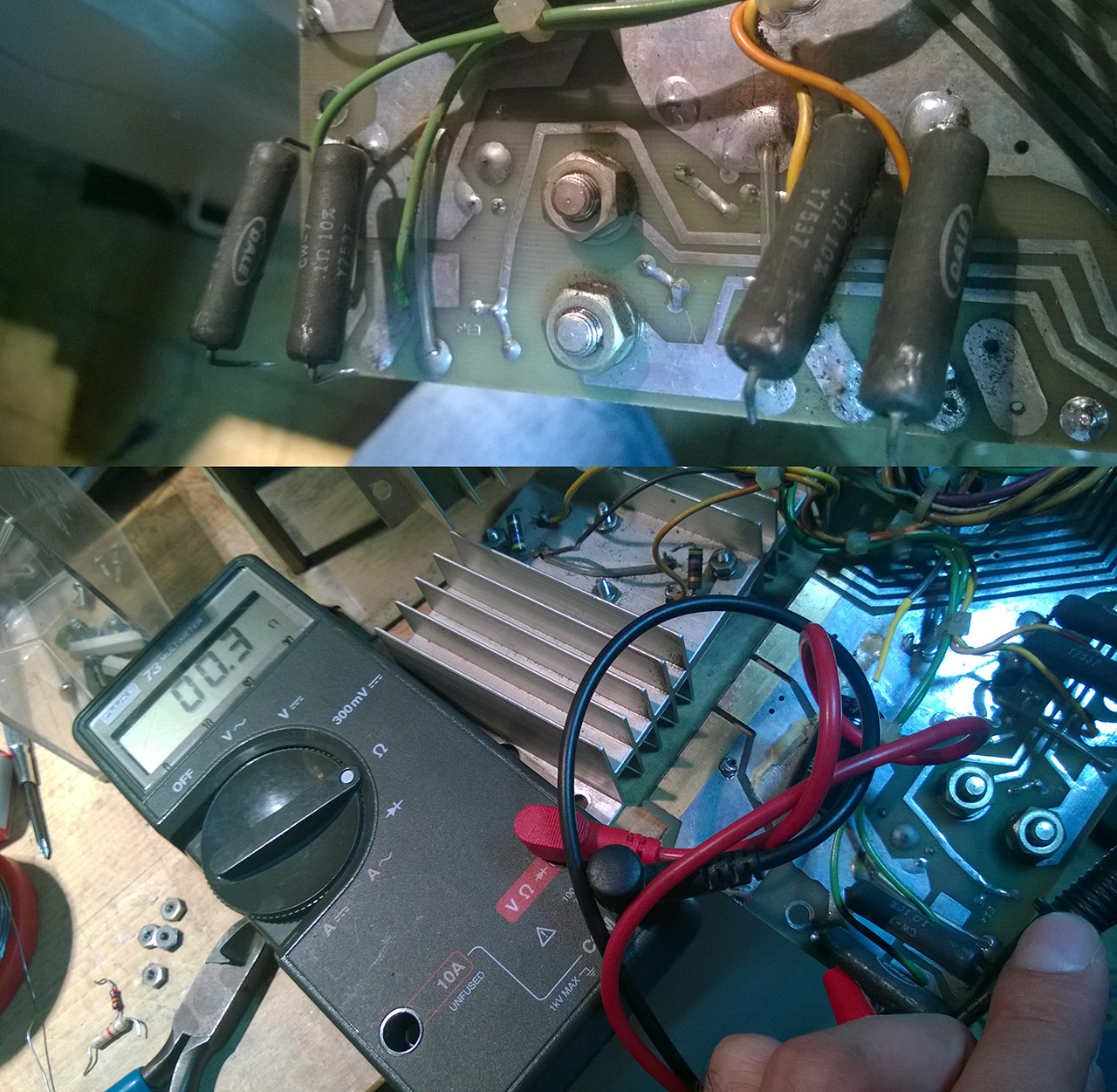
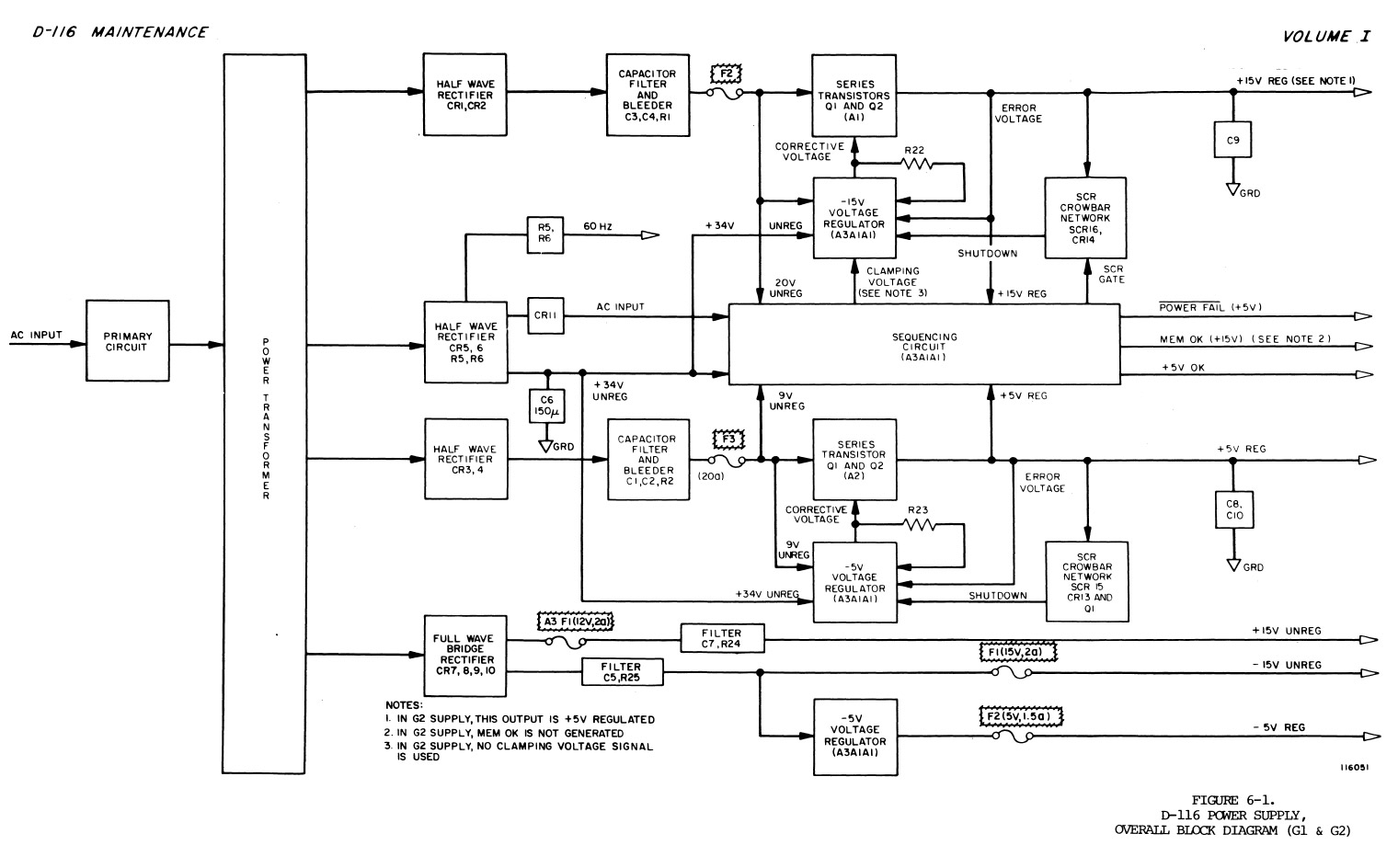
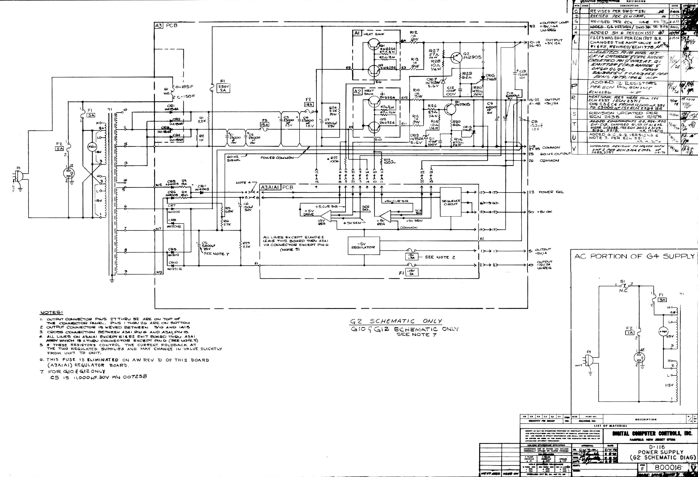
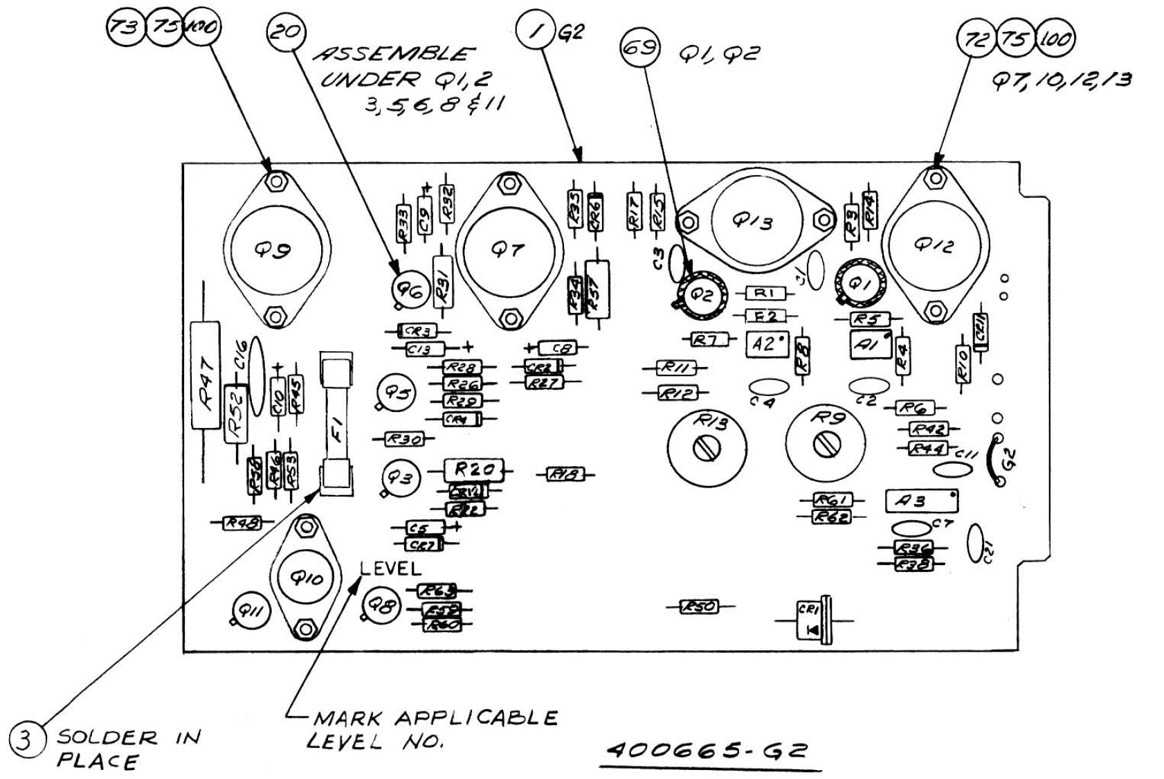
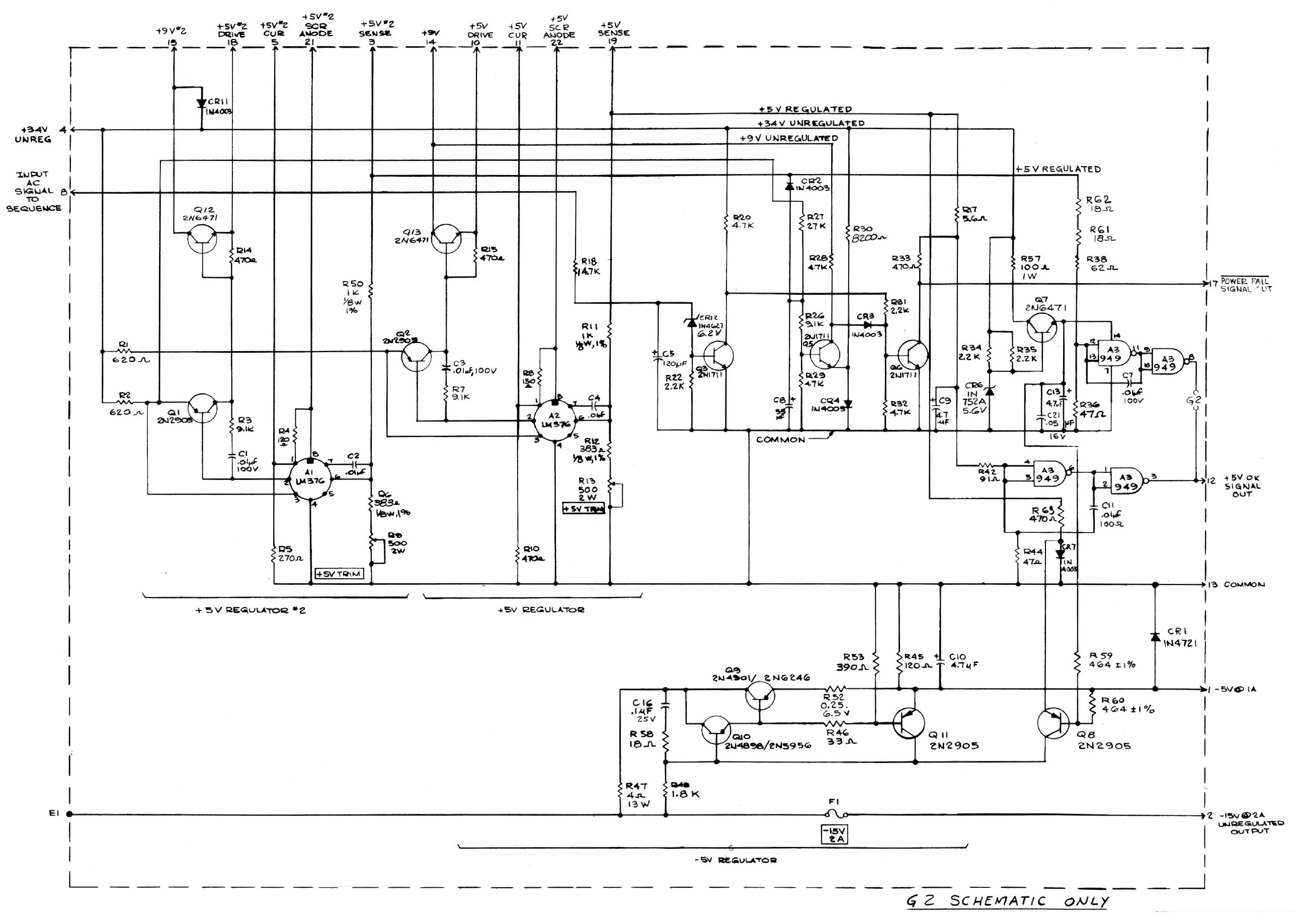
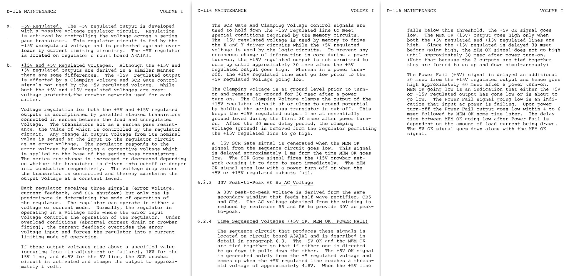
On Mon, Aug 21, 2017 at 11:47 AM Dominique Carlier via cctalk < [email protected]> wrote: > > Thank you very much for these valuable detailed information! :-) > > Also following the suggestions of Curious Marc, I focus now on the > comparison between the two almost identical circuits that deliver the > regulated + 5V on G2. > > Following your explanations, I started by checking the transistors and > resistors on the heatsinks A1 and A2, and also checking the resistors of > 0.1 Ω (R10 to R13) > > http://www.zeltrax.com/classiccmp_forum/psu_g2_test/cheked.jpg > > But first I see on the schematic that these transistors are supposed to > be "2N6254", but I see on A1 and A2 that the 4 transistors are "7540" > (full name: POWER PHYSICS 001554 7540), I do not find The datasheet of > this model. > > > http://www.zeltrax.com/classiccmp_forum/psu_g2_test/serie_pass_transistor.jpg > > The results of the test on the pass transistors: > By doing the various checks between B E C for NPN transistor, no > problems. No unwanted open or closed circuit at wrong place. > However if I measure the value between B and E, on all the transistors I > read + - 0.510 except for one where it is + -0.440, it is Q2 on A1 which > is precisely the board that delivers the + 5V which collapse. Is this > transistor defective? > > The small resistances which are between the bases and collectors of each > transistors all show + -50 Ω (they are supposed to be 47 Ω but I imagine > it's OK like that) > But about R10, R11, R12 and R13, these resistors are supposed to be have > a value of 0.1 Ω , right? > Because for these 4 resistors I read values ranging from 0.2 to 0.4 Ω! > > http://www.zeltrax.com/classiccmp_forum/psu_g2_test/resistor_check.jpg > > Strange thing, today I take the measurements again (with two different > multi-meters to be sure) and the values today are different, located > between 0.8 and 1 Ω !! I do not understand this variation, I had > unwrapped only one leg, I removed both now, same type of result: 0.9 Ω ! > > Unfortunately because these 4 resistors are in the same state, these are > probably not the cause of the collapsed +5V only on the side of A1, What > is your opinion about that? > Anyway, I'm going to change those resistors for sure. I will also change > the transistor which only passes 0.44 instead of 0.52, I intend to put > an equivalent of 2N6254 hoping that the actual 7540 are also an > equivalent of the 2N6254 mentioned in the schematics. > > Thanks a lot for your help ! > > Dominique > > On 20/08/2017 09:08, Brent Hilpert wrote: > > On 2017-Aug-19, at 12:10 PM, Dominique Carlier via cctalk wrote: > >> Maybe it's better to give us all the useful information these power > supplies, moreover it might be useful to other people with the same > computer. > >> > >> An overall bloc diagram of the D-116 power supply including G1 and G2. > >> http://www.zeltrax.com/classiccmp_forum/psu_overall_bloc_diagram.jpg > >> > >> The complete schematics of the part of the power supply named G2. > >> http://www.zeltrax.com/classiccmp_forum/g2_schematics.jpg > >> > >> A drawing of the regulation board of the power supply G2 with the > physical locations of the components. > >> http://www.zeltrax.com/classiccmp_forum/g2_regulator_board.jpg > >> > >> The schematics of this regulation board. > >> > http://www.zeltrax.com/classiccmp_forum/g2_regulator_board_schematics.jpg > >> > >> And a bit of literature concerning the principle of operation about the > regulation with this PSU (you will understand better why I am a little bit > lost ;-) This principle of regulation with a panoply of verification and > Protection systems everywhere is unusual for me) > >> http://www.zeltrax.com/classiccmp_forum/psu_regulation_principe.jpg > >> > >> I have already tried without the CPU board: same symptoms. Next step, > try to check the capacitors in operation. > >>> Results of the observations: > >>> - This is definitely the regulated +5V of the G2 power supply. More I > add boards more the + 5v level goes down. +5v, +4.8v, +3.6v, +2.9v. It > remains stable however with just the CPU and the three core memory boards, > it becomes difficult for the power supply when I add boards in addition to > these. > >>> - This is definitely not a problem at the level of the Power Fail > circuit. > >>> - The big capacitors are not in fault (I rechecked twice). > >>> - So this maybe a problem at the level of the regulation itself, the > +5V balancing system ? > >>> > >>> Question: a faulty voltage regulator can behave in this way? I always > thought it worked or it did not work, but not between the two states > depending on the charge. > > (In answer to the question, yes, a faulty regulator can produce > 'in-between' output voltage.) > > > > As is typical for power supplies of this type and era, this power supply > includes current limiting circuitry. > > > > The current-limiting circuitry will throttle down the output voltage > (not shut it off completely) as the output current draw goes above a design > limit. > > This would appear to fit the symptoms you describe. > > > > The current-limiting circuitry works by placing a small-value resistor > in the current path after the main regulator transistor(s) (aka pass > transistors) but prior to the voltage-regulation sense point. > > A transistor senses the voltage across this R. > > As the output current increases, the voltage across the current-sense R > increases, at some point the transistor starts to turn on, and the > transistor is connected in such a way that as it turns on it reduces the > drive to the pass transistors, throttling down the output voltage. > > > > Arbitrarily using the "A2" heatsink half of the two +5 supplies in this > power supply for component references, the current-sense R is comprised of > a series-parallel circuit formed by the BE junctions of the 2 pass > transistors (A2.Q1, A2.Q2), the two 0.1ohm Rs on the emitters of the pass > transistors (A3.R10,A3.R11), the 47ohm Rs between B&E of those transistors, > A3.R23, A3A1A1.R8, 376.R9, along with additional influence by 376.R8 and > A3A1A1.R10. > > The current sense transistor is inside the LM376 (see internal > schematic), 376.Q16 between pins 1 & 8, controlling the 1st-stage driver > transistor 376.Q14. > > > > There are various things that could go wrong on this circuitry. > > Anything that upsets the current-sense resistance network to cause the > net R to increase will lower the output current that can be drawn (that is, > the current limiting circuitry will start kicking in too 'early'). > > > > A likely scenario is one of the pass transistors has failed open. > > This would take out a parallel leg of the current-sense resistance. > > All current would be forced through the good pass transistor and it's > emitter resistor, raising the current-sense voltage for a given output > current. > > The current-limiting circuitry would kick in at a lower current than the > design intention. > > This is beneficial inasmuch as it would work to save the good pass > transistor. > > > > The 0.1 ohm 9W emitter resistors are critical, although they're probably > wirewound and fairly reliable unless quite overstressed. > > One of these resistors being open would result in the same operation as > an open pass transistor. > > You'll have difficulty measuring them with accuracy but you could do > some sanity checks for continuity around both the pass transistor circuit > legs, > > as well as checking the pass transistor BC/BE junctions. > > > > (In principle, the 'proper' thing to do in this area is look at what the > current-sense voltage is doing, but that requires knowing what the target V > is. Could compare with the other half of the supply.) > > > > None of this is to suggest this area is necessarily at fault, or rule > out other areas of the supply. > > > > Another possible fault that would fit the symptom (decreasing voltage as > current draw increases, if that's what's going on) is inadequate (partially > failed) drive to the pass transistors. > > In short, anything reducing the power gain of the regulator error > amplifier could produce this symptom. > > > > > > -- -- Anders Nelson +1 (517) 775-6129 www.erogear.com