Dominique,
I wouldn't worry about the readings on your 0.1 Ohm resistor, you are not going
to get any trustable results on something that low without a four wire
ohm-meter.
It seems that you have eliminated the power transistors as being the source of
the failure.
I'd like to eliminate the rectifier diodes or the big caps as the source of the
problem
1-        Could you please measure and compare (or better get a scope trace) of
the voltage at the F3 and F2 fuses when the voltage drops. If the voltage also
drops at the fuse (pre-regulation) then either your caps/diode combo is not
good, or your boards are drawing too much current.
2-       If that's the case, you could also easily swap the power source for
the two regulators. Temporarily lifting both fuses on the output side , and
cross wire F2 to feed A2 and F3 to feed A1. If the fault moves, that would
strongly  indicate that one of the cap/diode combo is bad. If it does not, then
either the regulation circuitry is bad or the boards draw an anomalous amount
of power.
3-       Measure how much each board is pulling (as far as amps). You can do
this easily by removing the fuse and putting an ammeter in its place, then plug
each board one at a time, and read what the amperage is.
4-       Do a similar measurement adding boards one by one and see at which
amperage the voltage starts to degrade, and if it exceeds the design criterion
for the power supply.
Marc
From: cctalk <[email protected]> on behalf of "[email protected]" <[email protected]>
Reply-To: Dominique Carlier <[email protected]>, "[email protected]"
<[email protected]>
Date: Wednesday, August 23, 2017 at 6:17 AM
To: "[email protected]" <[email protected]>
Subject: Re: DCC-116 E / DATA GENERAL NOVA 2/10 / Nixdorf 620 - Restoring and
restarting
Here is the situation.
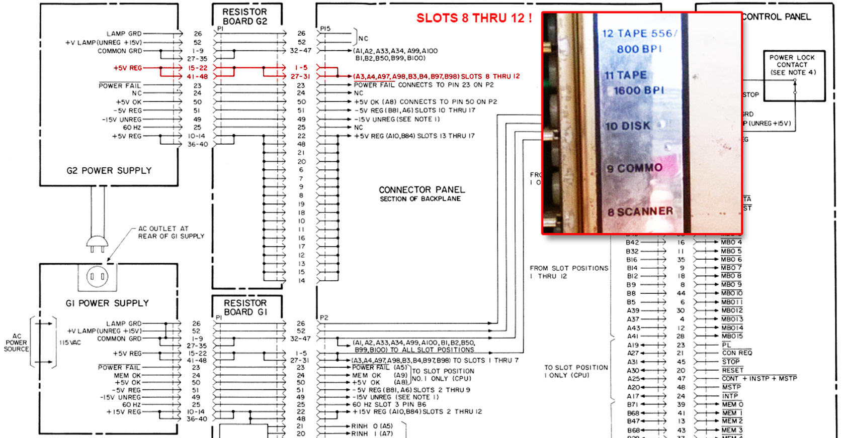
The + 5V 12A that collapses comes out from pins 10-14 / 36-40, the other
+ 5V 12A (pins 15-22 / 36-40) never goes down.
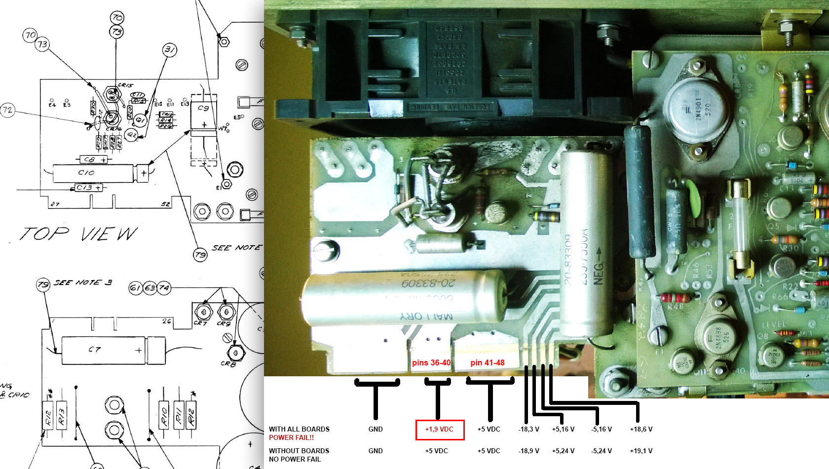
All that I surrounded in green on that image (1950×2361, zoomable) are
the components that I tested on the power supply G2, A3 motherboard,
regulation board and heatsink A1 + A2:
http://www.zeltrax.com/classiccmp_forum/psu_g2_test/g2_tested_components.jpg
To eliminate some doubts and because I do not have some spare parts on
hand, I switched the modules A1 and A2, same result. Idem with the
transistors 2N2905, same result.
The result is always the same : it's always the +5V on pins 10-14 /
36-40 that collapses, never the other output.
Some resistors are not yet tested is because these must be de-soldered
for a valid test, but the printed circuit is very fragile and many
component have legs bent into the weld.
Except for the not tested components (among others the LM376, the
rectifier diodes) At this stage I start again to suspect a little
everything. The famous large capacitors of the power supply (C1 to C4).
But also a possible problems on the boards of the computer itself.
As one of you mentioned, the hypothesis of shorted decoupling capacitors
on the boards could put the power supply in default.
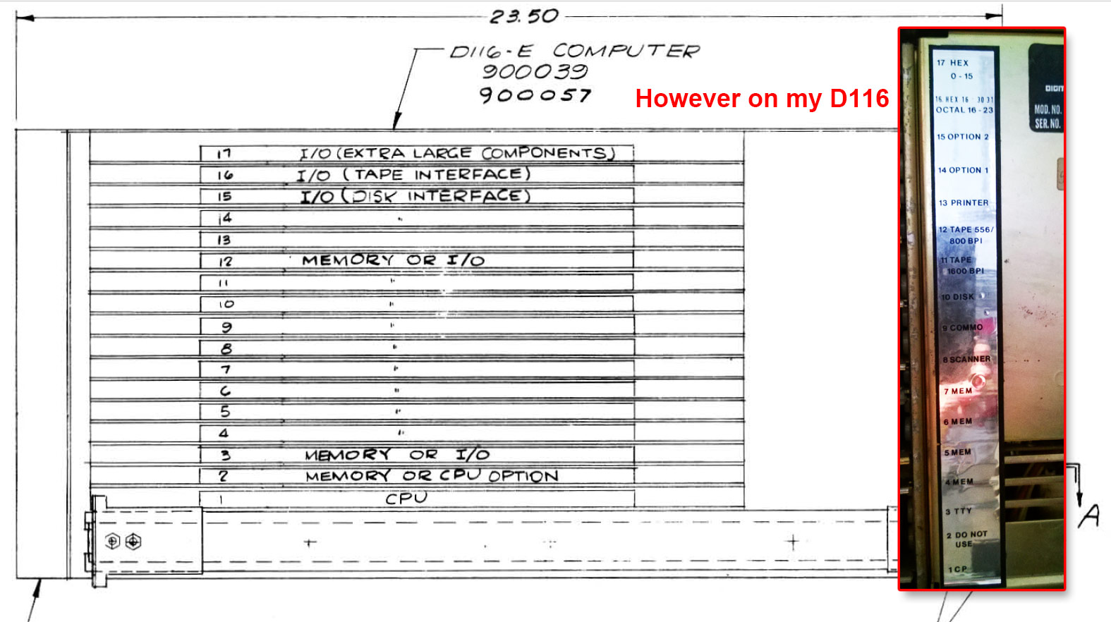
Note that the machine runs normally with the CPU board, three core
memory boards (400w each) + two multiplexing boards for terminals + the
printer board.
If I add only one of these remaining board:
- Disk Pack Controller
- 9-track tape Controller
- "scanner" board (also for terminals)
-> Power Fail.
Note that : if I only connect the CPU and the disk pack controller card:
Power Fail too !!
What makes me doubtful about this scenario is that I can not imagine
that these three boards, each causing the Power Fail, could fail
simultaneously. Remember that the first time I powered up the beast (one
big hour), the machine was working with all the boards and Power Fail
appeared at once.
I have not retested since but also note that by adding an external power
supply just for the deficient + 5V , the machine has restarted and even
booted the operating system.
If you have another ideas? LM376?
Thanks
Dominique
On 20/08/2017 09:08, Brent Hilpert wrote:
On 2017-Aug-19, at 12:10 PM, Dominique Carlier via cctalk wrote:
Maybe it's better to give us all the useful information these power supplies,
moreover it might be useful to other people with the same computer.
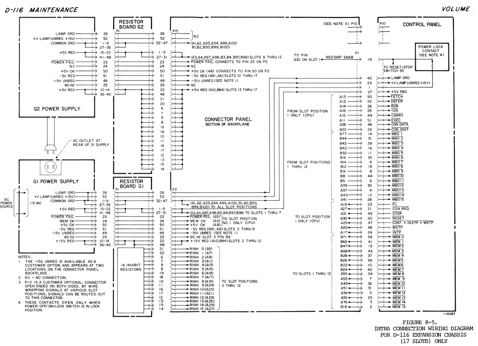
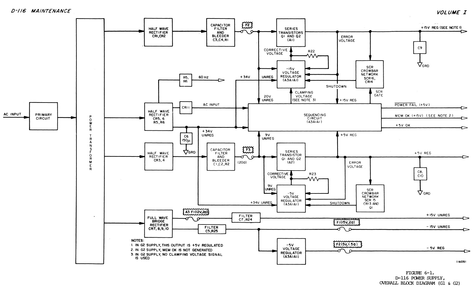
An overall bloc diagram of the D-116 power supply including G1 and G2.
http://www.zeltrax.com/classiccmp_forum/psu_overall_bloc_diagram.jpg
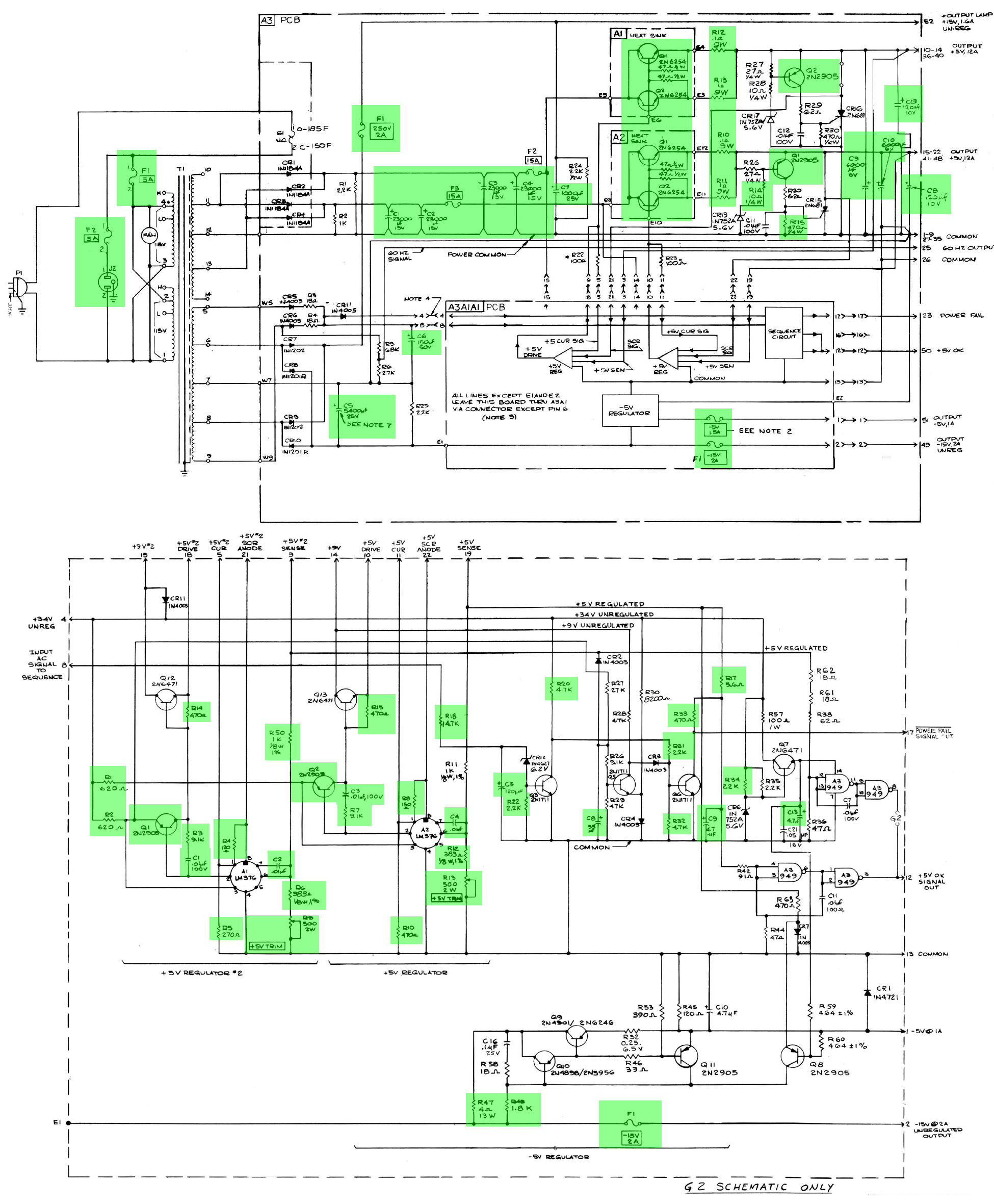
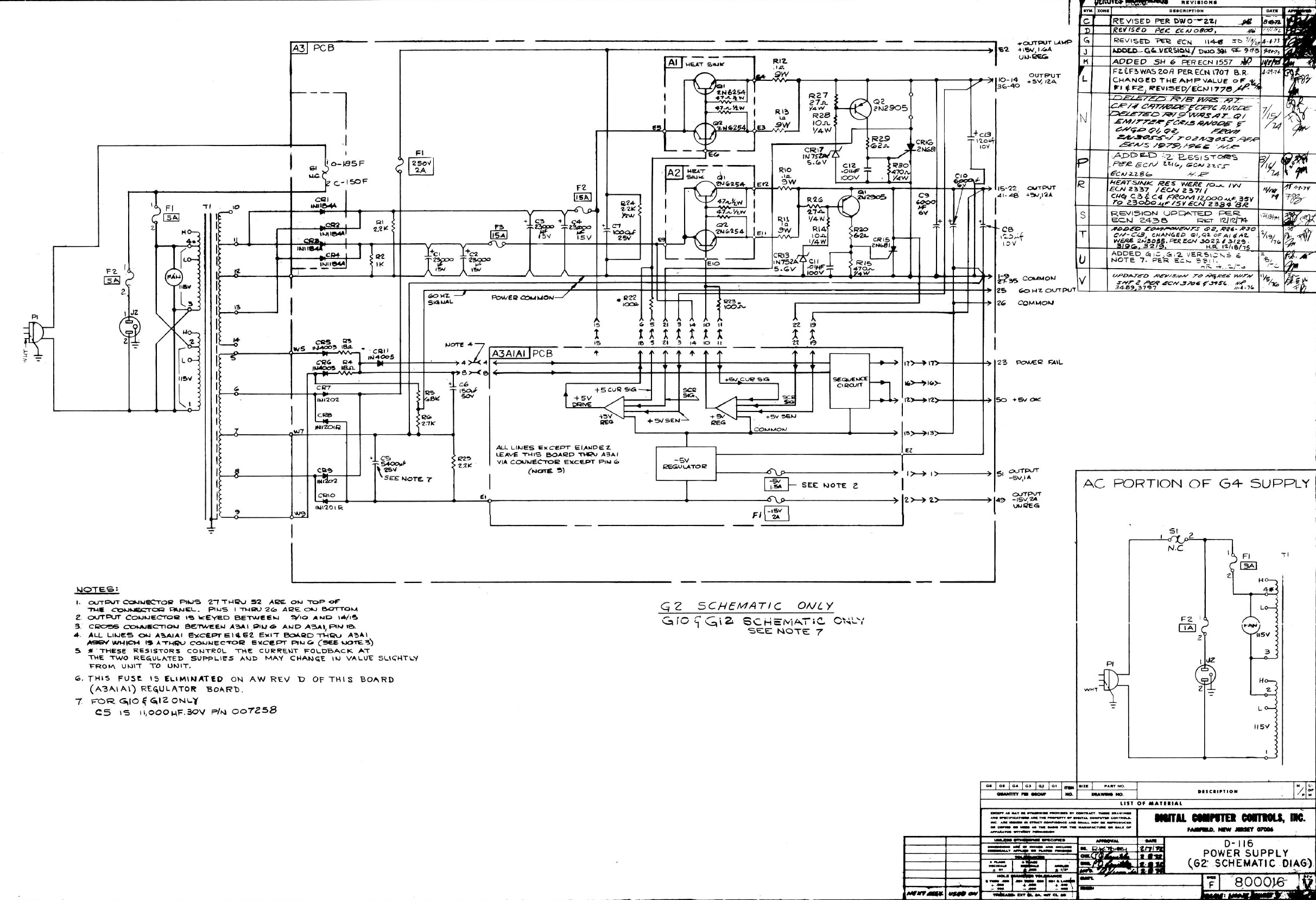
The complete schematics of the part of the power supply named G2.
http://www.zeltrax.com/classiccmp_forum/g2_schematics.jpg
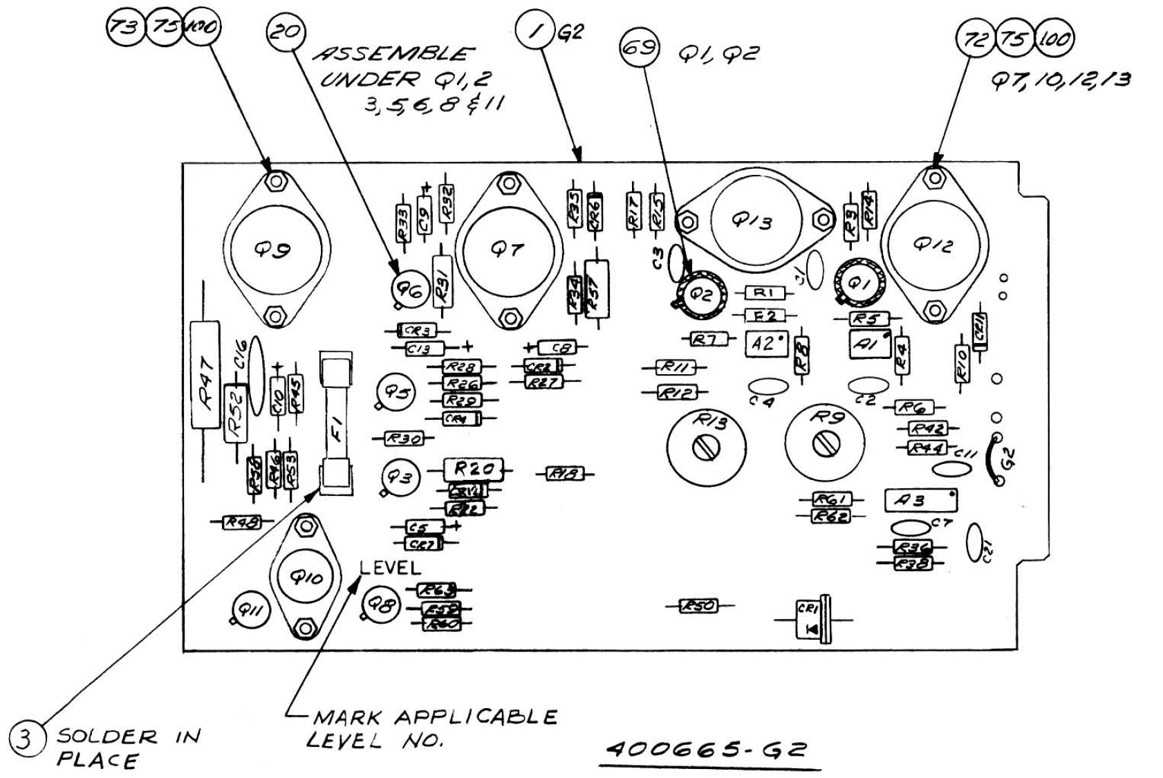
A drawing of the regulation board of the power supply G2 with the physical locations of the components.
http://www.zeltrax.com/classiccmp_forum/g2_regulator_board.jpg
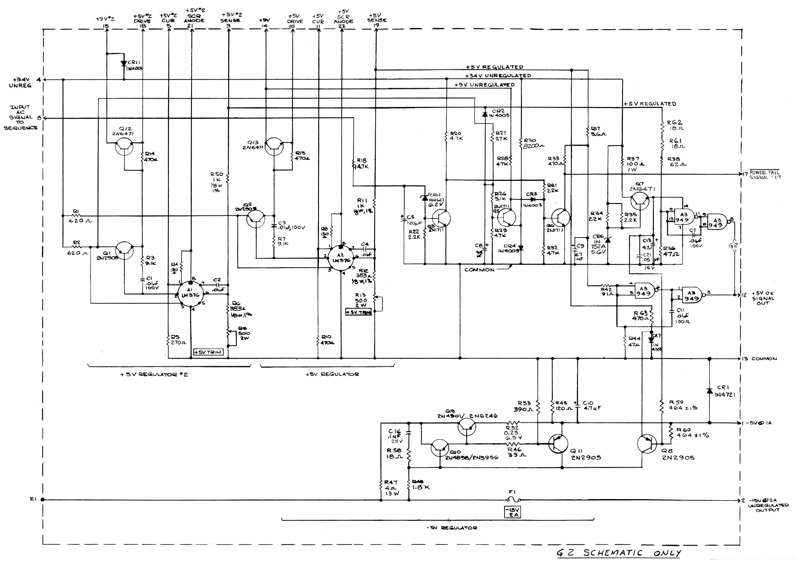
The schematics of this regulation board.
http://www.zeltrax.com/classiccmp_forum/g2_regulator_board_schematics.jpg
And a bit of literature concerning the principle of operation about the regulation with this PSU (you will understand better why I am a little bit lost ;-) This principle of regulation with a panoply of verification and Protection systems everywhere is unusual for me)
http://www.zeltrax.com/classiccmp_forum/psu_regulation_principe.jpg
I have already tried without the CPU board: same symptoms. Next step, try to check the capacitors in operation.
Results of the observations:
- This is definitely the regulated +5V of the G2 power supply. More I add
boards more the + 5v level goes down. +5v, +4.8v, +3.6v, +2.9v. It remains
stable however with just the CPU and the three core memory boards, it becomes
difficult for the power supply when I add boards in addition to these.
- This is definitely not a problem at the level of the Power Fail circuit.
- The big capacitors are not in fault (I rechecked twice).
- So this maybe a problem at the level of the regulation itself, the +5V
balancing system ?
Question: a faulty voltage regulator can behave in this way? I always thought it worked or it did not work, but not between the two states depending on the charge.
(In answer to the question, yes, a faulty regulator can produce 'in-between'
output voltage.)
As is typical for power supplies of this type and era, this power supply includes current limiting circuitry.
The current-limiting circuitry will throttle down the output voltage (not shut it off completely) as the output current draw goes above a design limit.
This would appear to fit the symptoms you describe.
The current-limiting circuitry works by placing a small-value resistor in the current path after the main regulator transistor(s) (aka pass transistors) but prior to the voltage-regulation sense point.
A transistor senses the voltage across this R.
As the output current increases, the voltage across the current-sense R
increases, at some point the transistor starts to turn on, and the transistor
is connected in such a way that as it turns on it reduces the drive to the pass
transistors, throttling down the output voltage.
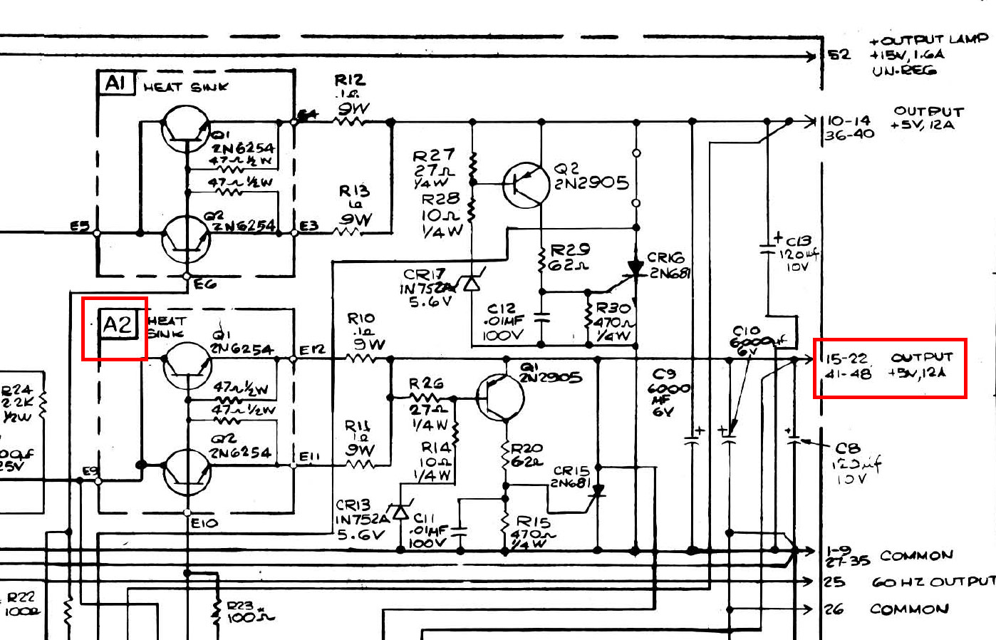
Arbitrarily using the "A2" heatsink half of the two +5 supplies in this power supply for component references, the current-sense R is comprised of a series-parallel circuit formed by the BE junctions of the 2 pass transistors (A2.Q1, A2.Q2), the two 0.1ohm Rs on the emitters of the pass transistors (A3.R10,A3.R11), the 47ohm Rs between B&E of those transistors, A3.R23, A3A1A1.R8, 376.R9, along with additional influence by 376.R8 and A3A1A1.R10.
The current sense transistor is inside the LM376 (see internal schematic), 376.Q16
between pins 1 & 8, controlling the 1st-stage driver transistor 376.Q14.
There are various things that could go wrong on this circuitry.
Anything that upsets the current-sense resistance network to cause the net R to
increase will lower the output current that can be drawn (that is, the current
limiting circuitry will start kicking in too 'early').
A likely scenario is one of the pass transistors has failed open.
This would take out a parallel leg of the current-sense resistance.
All current would  be forced through the good pass transistor and it's emitter
resistor, raising the current-sense voltage for a given output current.
The current-limiting circuitry would kick in at a lower current than the design
intention.
This is beneficial inasmuch as it would work to save the good pass transistor.
The 0.1 ohm 9W emitter resistors are critical, although they're probably wirewound and fairly reliable unless quite overstressed.
One of these resistors being open would result in the same operation as an open
pass transistor.
You'll have difficulty measuring them with accuracy but you could do some
sanity checks for continuity around both the pass transistor circuit legs,
as well as checking the pass transistor BC/BE junctions.
(In principle, the 'proper' thing to do in this area is look at what the current-sense voltage is doing, but that requires knowing what the target V is. Could compare with the other half of the supply.)
None of this is to suggest this area is necessarily at fault, or rule out other areas of the supply.
Another possible fault that would fit the symptom (decreasing voltage as current draw increases, if that's what's going on) is inadequate (partially failed) drive to the pass transistors.
In short, anything reducing the power gain of the regulator error amplifier
could produce this symptom.